
Weight Optimized Stiffener and Sealing Structure for Direct Liquid Cooled Modules

a liquid cooled module and stiffener technology, applied in cooling/ventilation/heating modification, semiconductor device details, semiconductor devices, etc., can solve the problems of high power heat sources in servers, likely require large compute resources at a high density, and achieve the effect of reducing its thermal mass

Active Publication Date: 2021-11-25
GOOGLE LLC
View PDF16 Cites 0 Cited by
  • Summary
  • Abstract
  • Description
  • Claims
  • Application Information

AI Technical Summary

Benefits of technology

The present patent provides a stiffener that helps control warping of a lidless package and allows direct liquid cooling of a chip or substrate. The stiffener is made with weight optimization material and has geometric features that further reduce its weight. This improves the stiffener's attachment to a circuit assembly by reducing its thermal mass and impact from weight concentration.

Problems solved by technology

In addition to industry standard chip packages, the exploration of special purpose silicon is likely to result in high power heat sources in servers.
Further, services such as imaging and artificial intelligence (“AI”) will likely require large compute resources at a high density, with many servers in close proximity to one another.

Method used


Image

  • Weight Optimized Stiffener and Sealing Structure for Direct Liquid Cooled Modules
  • Weight Optimized Stiffener and Sealing Structure for Direct Liquid Cooled Modules
  • Weight Optimized Stiffener and Sealing Structure for Direct Liquid Cooled Modules

Examples


Embodiment Construction

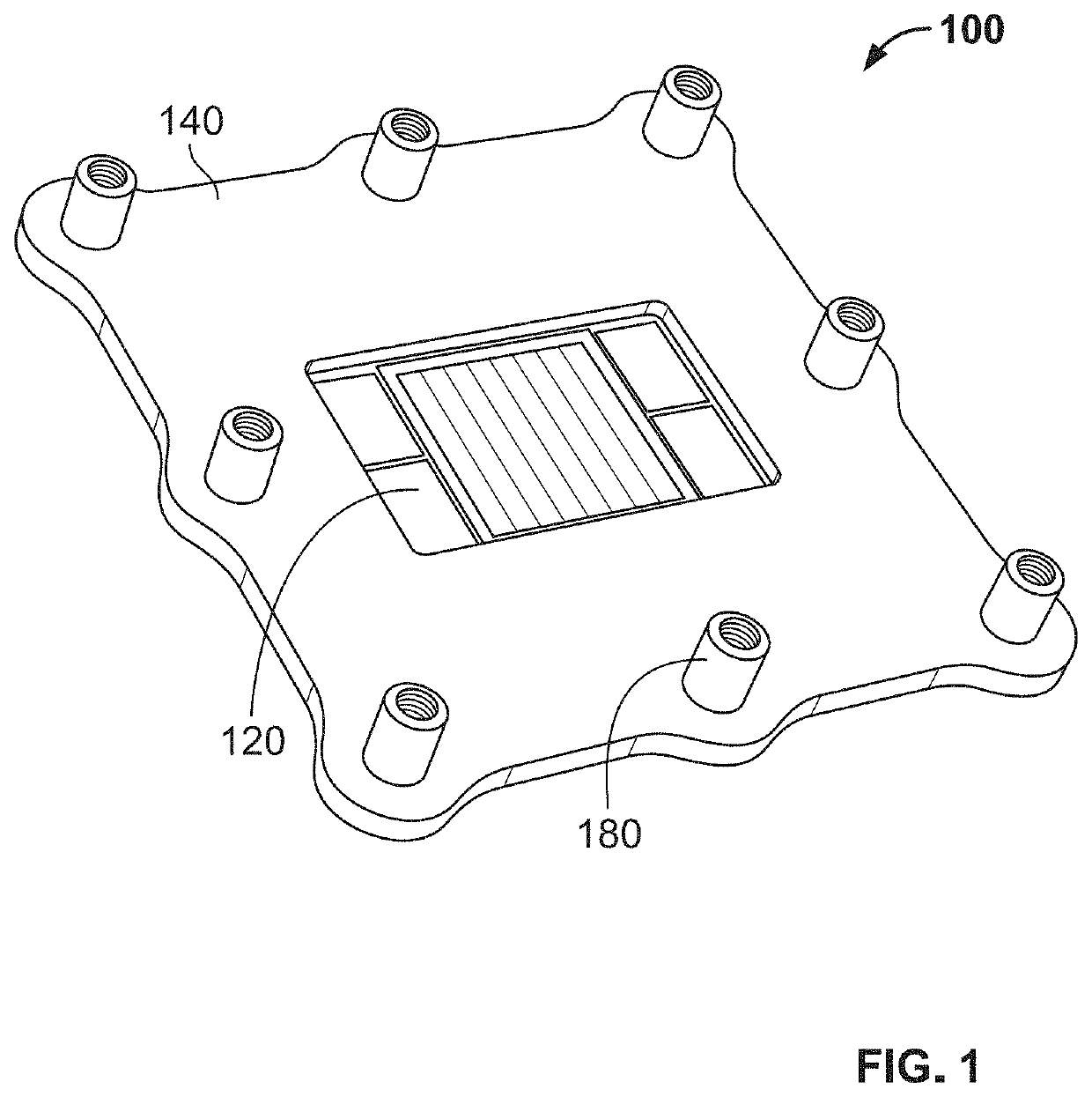
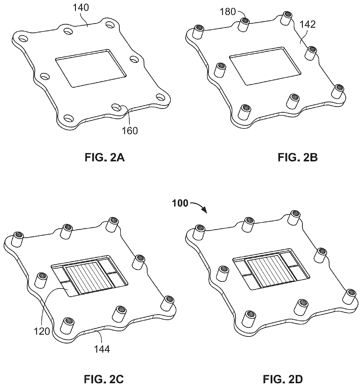
[0022]FIG. 1 is a perspective view of a package subassembly 100 of a semiconductor device including a substrate 120 bonded to stiffener 140 with fasteners or threaded hardware 180 installed thereto.

[0023]The stiffener 140 has a top surface, a bottom surface and an aperture through the top and bottom surfaces. The aperture may be generally central with respect to an outer perimeter of the stiffener 140, though in other examples the position of the aperture may be adjusted. For example, the size and shape and position of the aperture may be adapted based on circuitry of the underlying substrate 120 to be exposed through the aperture.

[0024]The substrate 120 may be coupled to the bottom surface of the stiffener, such as by an adhesive or other bonding techniques. A portion of stiffener 140 may cover a portion of the substrate 120 when the substrate is coupled to the bottom surface of the stiffer. For example, the substrate may include circuitry on a least a first region on its top surfa...


PUM


Abstract

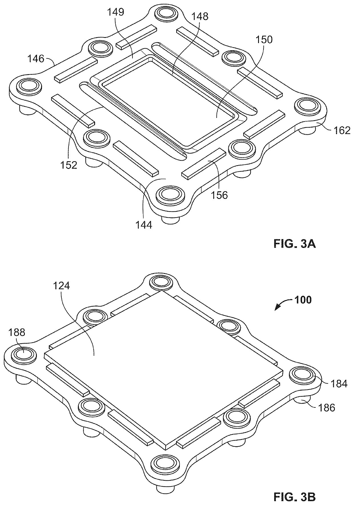
A weight optimized stiffener for use in a semiconductor device is disclosed herein. In one example, the stiffener is made of AlSiC for its weight and thermal properties. An O-ring provides sealing between a top surface of the stiffener and a component of the semiconductor device and adhesive provides sealing between a bottom surface of the stiffener and another component of the semiconductor device. The stiffener provides warpage control for a lidless package while enabling direct liquid cooling of a chip or substrate.

Description

BACKGROUND[0001]Complementary Metal Oxide Semiconductor (“CMOS”) circuits are found in several types of electronic components, including microprocessors, batteries, and digital camera image sensors. The main features of CMOS technology are low static power consumption and high noise immunity.[0002]In addition to industry standard chip packages, the exploration of special purpose silicon is likely to result in high power heat sources in servers. This technology may also be applied to graphics processing units (“GPUs”) and custom application-specific integrated circuits (“ASICs”). Further, services such as imaging and artificial intelligence (“AI”) will likely require large compute resources at a high density, with many servers in close proximity to one another. Data centers around the globe are being mandated to simultaneously increase energy efficiency, consolidate operations and reduce costs. To accommodate these high performance and high density servers, data center operators must...

Claims


Application Information

Patent Timeline
Patent Type & Authority Applications(United States)
IPC IPC(8): H01L23/00H01L23/16H01L23/473
CPCH01L23/562H01L23/473H01L23/16H01L23/32H01L23/4006H01L2023/4087H01L2023/405H05K7/20H01L23/36H01L23/367H01L23/04H01L25/04
Inventor IYENGAR, MADHUSUDAN K.BURGESS, CONNORJAIN, PADAMSAMADIANI, EMADLI, YUAN
Owner GOOGLE LLC
Learn More