

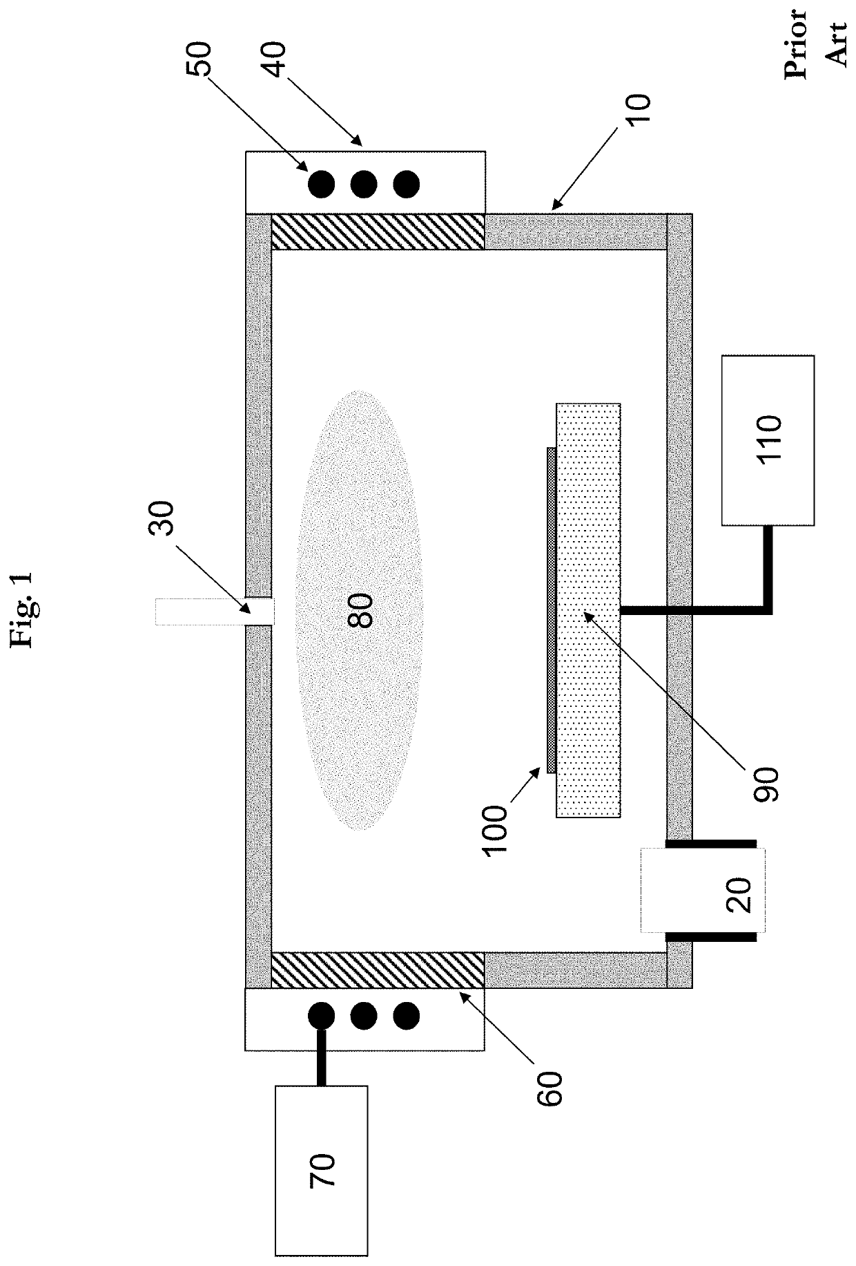
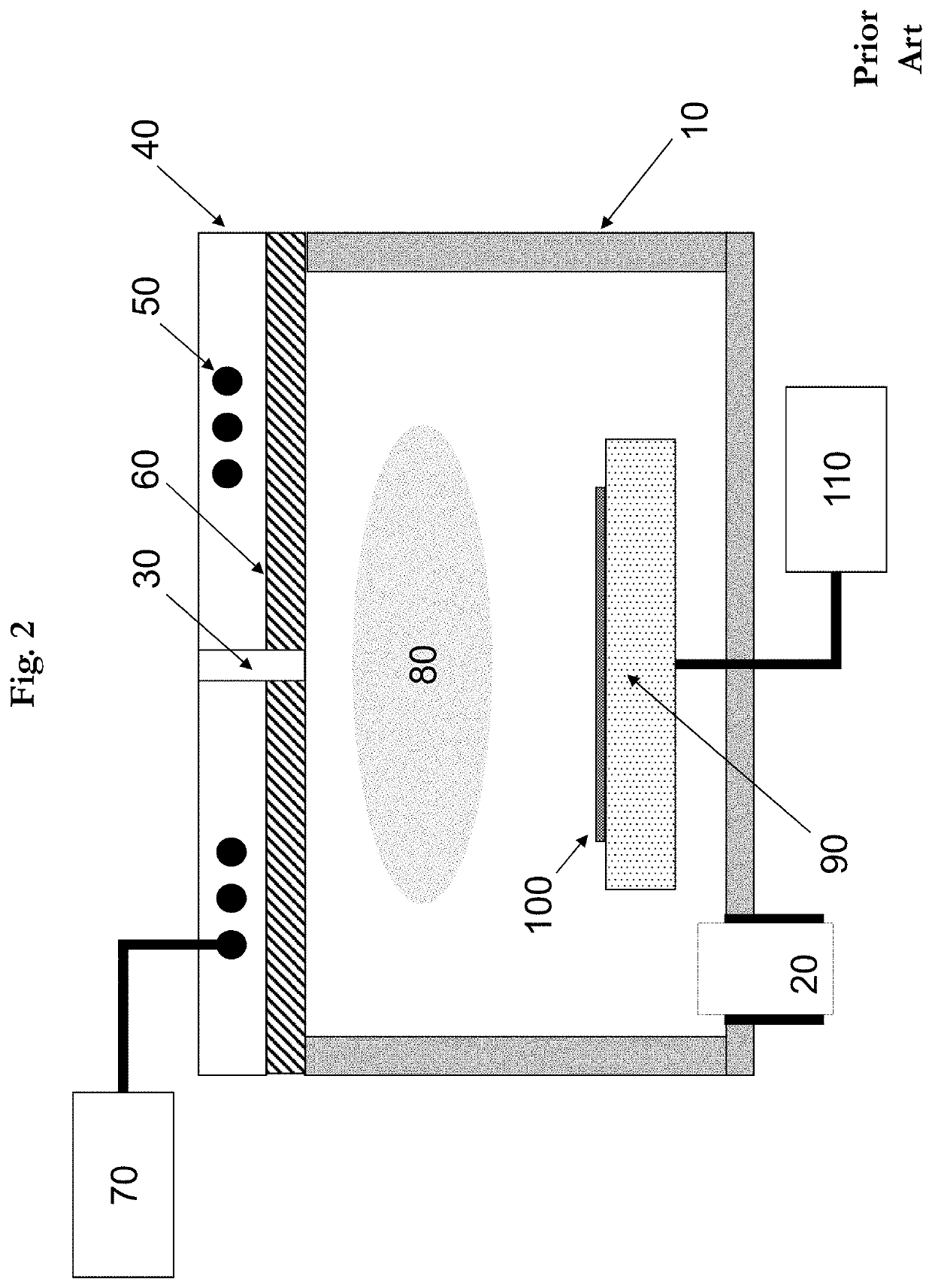
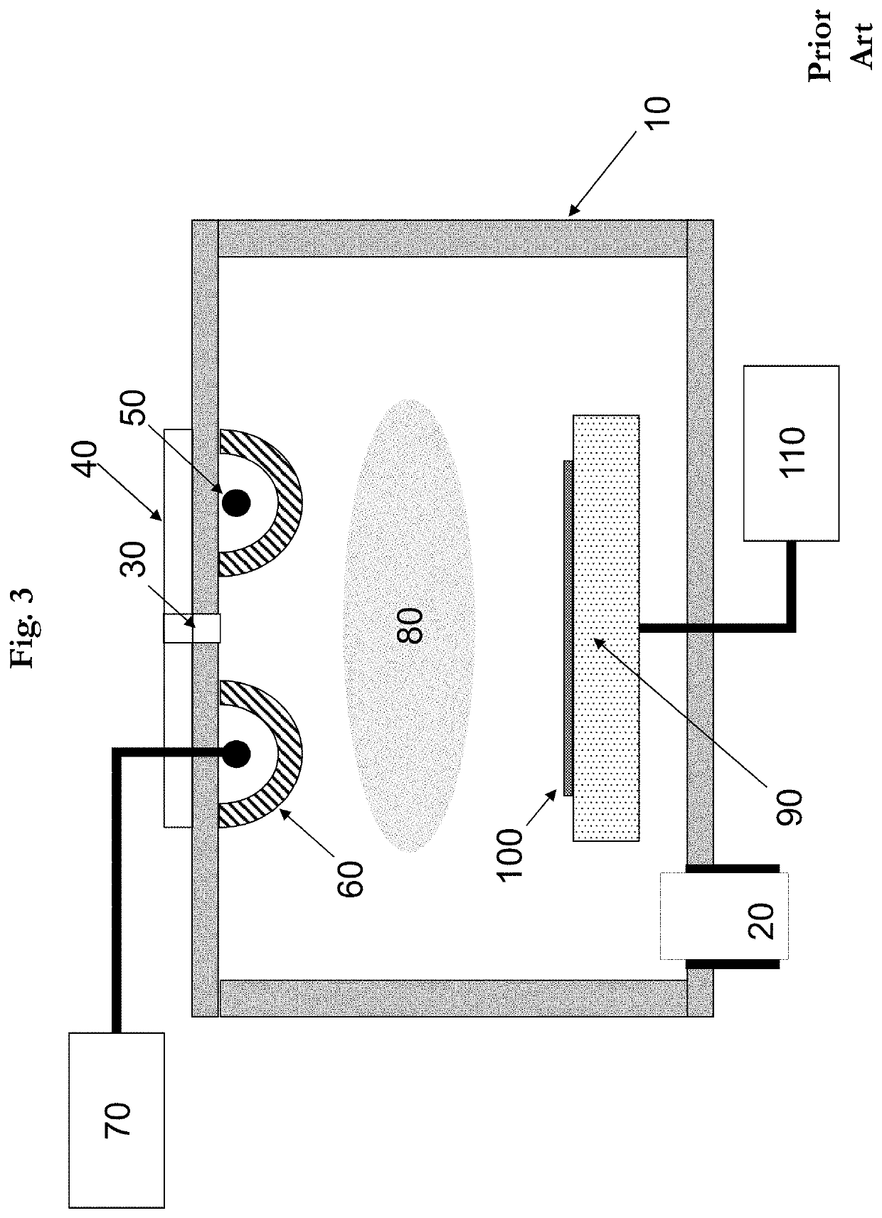
Plasma Source Configuration
a plasma source and configuration technology, applied in the direction of coatings, chemical vapor deposition coatings, electric discharge tubes, etc., can solve the problems of significantly reducing the ability of conductive materials, har structure can interfere with coupling rf energy, and conductive material buildup on the dielectric window, so as to achieve high aspect ratio gap
- Summary
- Abstract
- Description
- Claims
- Application Information
AI Technical Summary
Benefits of technology
Problems solved by technology
Method used
Image

Examples
Embodiment Construction
[0041]The present invention, according to one embodiment, provides a HAR film breaker wherein the HAR feature is formed by at least two components. These at least two components are sufficient to inhibit conductive material deposition in the HAR feature during the deposition of a thin film. When cleaning of the HAR film breaker is required, the HAR feature can be disassembled which provides for easy access to the interior surfaces of the HAR feature for the cleaning process. Thus, the manufacture of film breaker structures with very high aspect ratios (>10:1) according to the present invention allows for an easy to clean and maintain HAR film breaker.
[0042]In addition, the at least two components design is simpler to manufacture and reduces the cost of manufacturing the film breaker. Further, only a portion of the HAR surface is required to be electrically insulating. However, all of the HAR surfaces can be electrically insulating. The film breaker can contain conductive material (e...
PUM
| Property | Measurement | Unit |
|---|---|---|
| width | aaaaa | aaaaa |
| gap width | aaaaa | aaaaa |
| gap width | aaaaa | aaaaa |
Abstract
Description
Claims
Application Information