Process for depositing F-doped silica glass in high aspect ratio structures

a technology of fdoped silica glass and high aspect ratio, which is applied in the direction of vacuum evaporation coating, coating, plasma technique, etc., can solve the problems of increasing the signal propagation time through, adversely affecting circuit performance, and increasing the density of circuit elements and dimensions on wafers or silicon substrates, so as to reduce reducing sputtering components, and reducing the effect of sputtering

Inactive Publication Date: 2005-01-25
NOVELLUS SYSTEMS
View PDF15 Cites 27 Cited by
  • Summary
  • Abstract
  • Description
  • Claims
  • Application Information

AI Technical Summary

Benefits of technology

In accordance with the present invention, a high aspect ratio gap-fill process uses high density plasma (HDP) deposition processes with helium, hydrogen, or other inefficient sputtering gases, instead of argon to reduce the effects of sputtering and redeposition for depositing fluorine-doped films, such as FSG (F-doped silica glass). Because the sputtering agent is greatly reduced, the etch or sputter rate decreases and the facet moves away from the element corners, as expected. Cusps form to a lesser extent on the element sidewalls because much less material is etched and available for redeposition. Consequently, with a greatly reduced sputter component, gaps remain open longer so that higher aspect ratio gaps can be filled without the formation of voids. The gas mixture can include both hydrogen and helium in some embodiments.

Problems solved by technology

However, as semiconductor technology advances, circuit elements and dimensions on wafers or silicon substrates are becoming increasingly more dense.
As capacitance increases, the RC time delay increases, which decreases the frequency response of the circuit and increases the signal propagation time through the circuit, thereby adversely affecting circuit performance.
As a result, filling these narrower gaps becomes more difficult, which can lead to unwanted voids and discontinuities in the insulating or gap-fill material.
However, as shown in FIG. 4, filling higher gap aspect ratios results in voids 410 due to cusps 420 prematurely closing the gaps even if the etch / dep ratio is optimized to 1 at the element corners.
If the etch rate is increased to keep the gaps open longer, undesirable corner clipping can occur.

Method used


Image

  • Process for depositing F-doped silica glass in high aspect ratio structures
  • Process for depositing F-doped silica glass in high aspect ratio structures
  • Process for depositing F-doped silica glass in high aspect ratio structures

Examples


Embodiment Construction

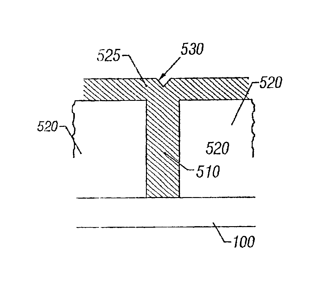
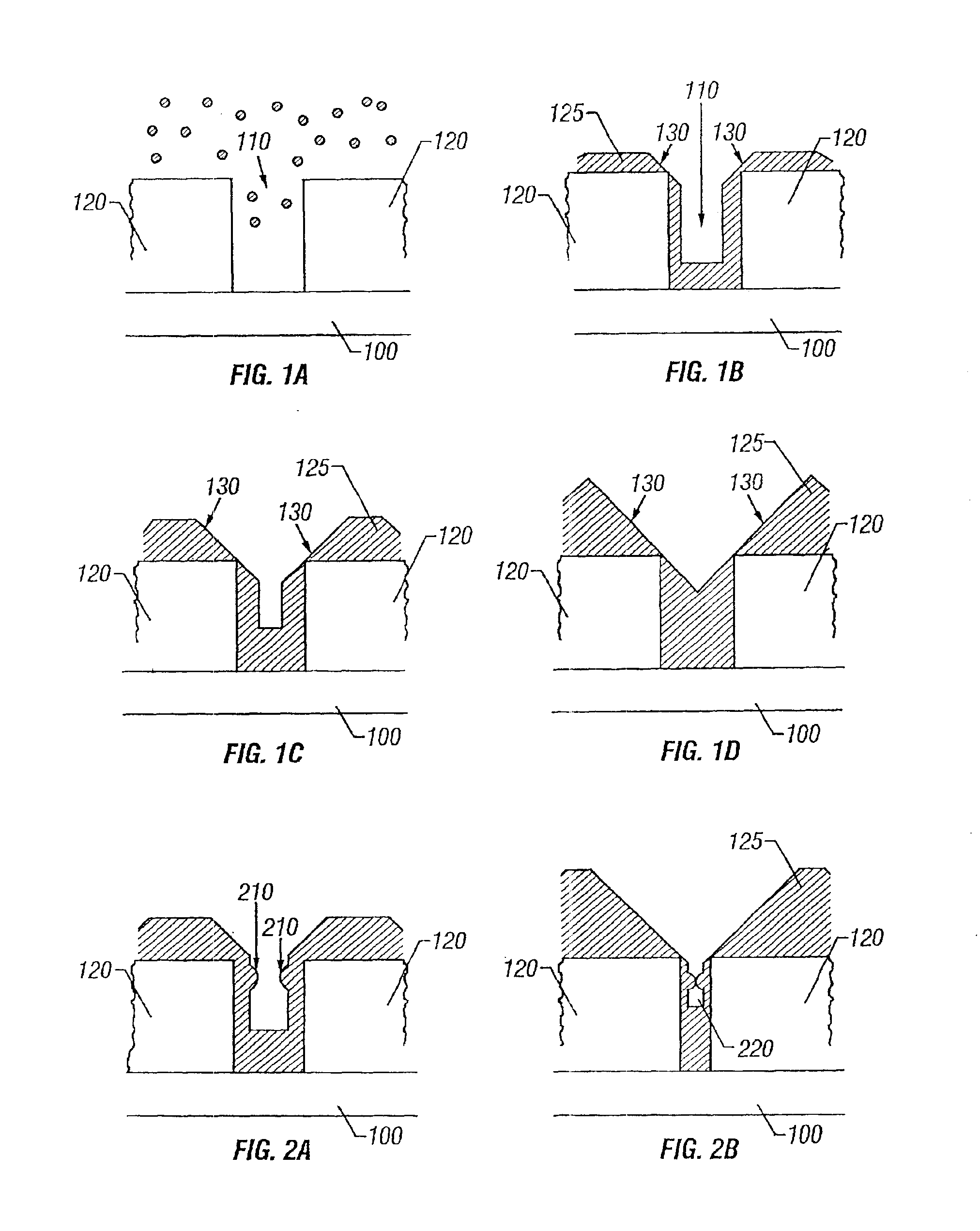
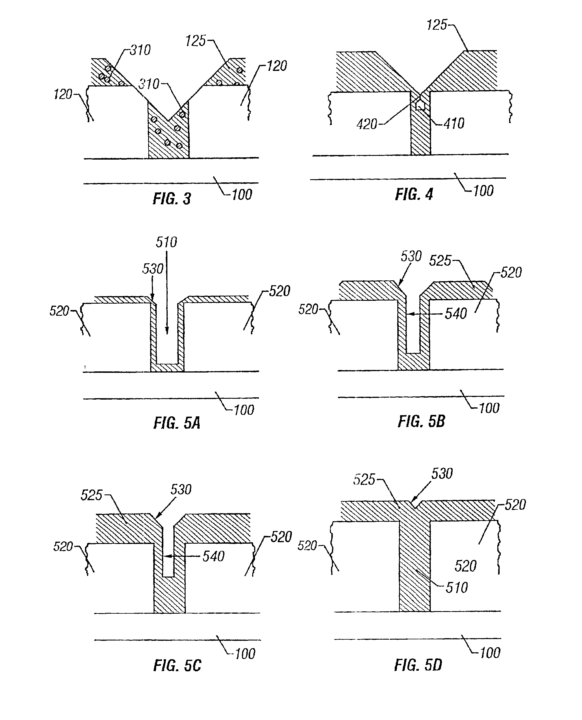
In accordance with an embodiment of the present invention, a process using high density plasma (HDP) deposition with helium, hydrogen, or other inefficient inert sputtering gases, is provided, which allows high aspect ratio gaps to be filled using fluorine-doped films without voids or clipped corners associated with conventional methods. In other embodiments, the gas mixture includes both helium and hydrogen.

Similar to conventional HDP deposition processes, a gas mixture is used containing silane (SiH4), a fluorine-bearing precursor, and oxygen (O2). However, contrary to conventional HDP processes, argon (Ar) is not used; rather an inefficient sputtering gas with an atomic weight lower than Ar is used, such as helium (He), hydrogen (H2), and / or neon (Ne). A mixture that includes SiH4, O2, a fluorine-bearing precursor, and hydrogen and / or He is used to simultaneously deposit and etch dielectric material, where SiH4, O2, and the fluorine-bearing precursor are used to form SiO2 for the...


PUM

PropertyMeasurementUnit
frequencyaaaaaaaaaa
frequencyaaaaaaaaaa
dielectric constantaaaaaaaaaa

Abstract

A process for filling high aspect ratio gaps on substrates uses conventional high density plasma deposition processes to deposit fluorine-doped films, with an efficient sputtering inert gas, such as Ar, replaced or reduced with an inefficient sputtering inert gas such as He and/or hydrogen. By reducing the sputtering component, sidewall deposition from the sputtered material is reduced. Consequently, gaps with aspect ratios greater than 3.0:1 and spacings between lines less than 0.13 microns can be filled with low dielectric constant films without the formation of voids and without damaging circuit elements.

Description

FIELD OF THE INVENTIONThe present invention relates generally to methods of thin film deposition and, particularly, to a process of filling high aspect ratio gaps on substrates using high density plasma (HDP) chemical vapor deposition (CVD).DESCRIPTION OF RELATED ARTIntegrated circuits fabricated on semiconductor substrates for large scale integration require multiple levels of metal interconnections to electrically interconnect the discrete layers of semiconductor devices on the semiconductor chips. The different levels of interconnections are separated by various insulating or dielectric layers, which have etched via holes to connect one level of metal to the next. Typically, the insulating layer is a silicon oxide having a dielectric constant k of approximately 4.1 to approximately 4.5.However, as semiconductor technology advances, circuit elements and dimensions on wafers or silicon substrates are becoming increasingly more dense. Consequently, the spacing between the metal line...

Claims


Application Information

Patent Timeline
Patent Type & Authority Patents(United States)
IPC IPC(8): C23C16/04C23C16/507C23C16/50H01L21/02H01L21/762H01L21/70H01L21/316
CPCC23C16/045C23C16/507H01L21/02129H01L21/76224H01L21/02274H01L21/31612H01L21/02164C23C16/401C23C16/509H05H1/02
Inventor PAPASOULIOTIS, GEORGE D.TAS, ROBERT D.VAN CLEEMPUT, PATRICK A.VAN SCHRAVENDIJK, BART
Owner NOVELLUS SYSTEMS
Why Eureka
Try Eureka