

Silica spherical particles for semiconductor sealing material
a technology sealing materials, which is applied in the field of silicon spherical particles, can solve the problems of greatly affecting the productivity and the cost, and affecting the heat dissipation effect, and achieves the effects of slow shear rate, relatively high flow velocity of the other overfill portion, and high shear ra
- Summary
- Abstract
- Description
- Claims
- Application Information
AI Technical Summary
Benefits of technology
Problems solved by technology
Method used
Image

Examples
examples
(Preparation of Silica Spherical Particles)
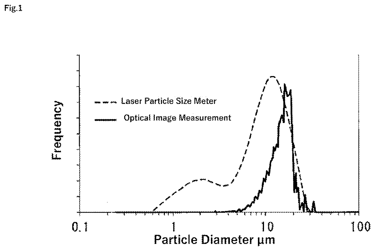
[0059]Crushed silica raw material was used to be spheroidized by thermal spraying method. The resulting particles were separated into coarse particles and fine particles by a cyclone, and as a result of the particle size measurement by the optical measurement on the coarse particle side, particles having D10 of 13.4 μm and D50 of 21.1 μm were prepared, and then sieved with an opening of 20 μm and collected only under the sieve. Silica fine powder having a specific surface area of 5 to 30 m2 / g was added thereto and the resulting mixture was mixed so that the volume ratio of the particles with a particle diameter of 1 μm or less as measured by the laser particle size measurement was 1.2% to prepare silica spherical particles.
(Measurement of Silica Spherical Particles)
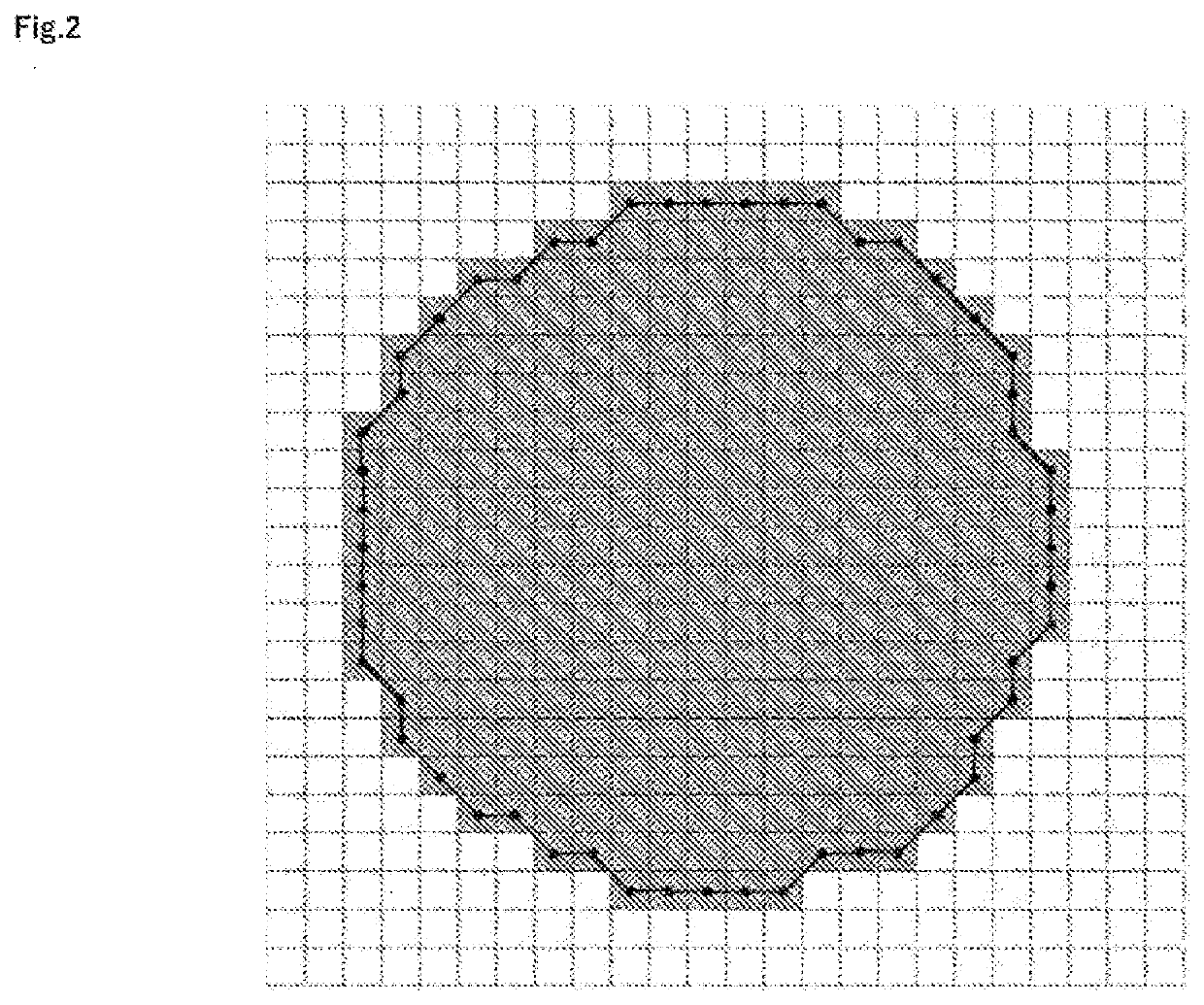
[0060]Dmode, D10, D50, D99, roundness, and slope n value (particle diameter 10-20 μm) of Rosin-Rammler diagram were obtained from the mixed silica particles by the above optical ...
PUM
| Property | Measurement | Unit |
|---|---|---|
| size | aaaaa | aaaaa |
| particle diameter | aaaaa | aaaaa |
| particle diameter | aaaaa | aaaaa |
Abstract
Description
Claims
Application Information