Flexible conductive film, producing method thereof, and display panel

a flexible conductive film and production method technology, applied in the field of optics, can solve the problems of high raw material cost of ito film, limited conductivity of ito film, and inability to bend the ito film, so as to improve the service life and improve the flexibility and stability of the conductive layer

Inactive Publication Date: 2022-01-20
TCL CHINA STAR OPTOELECTRONICS TECH CO LTD
View PDF0 Cites 0 Cited by
  • Summary
  • Abstract
  • Description
  • Claims
  • Application Information

AI Technical Summary

Benefits of technology

[0029]The present disclosure brings beneficial effects as follows. The method of producing the flexible conductive film provided by the present disclosure can improve the flexibility and the stability of the conductive layer while the conductive layer is being used, thereby improving the service life of the flexible conductive film.

Problems solved by technology

The technology of the ITO film is mature but the raw material cost of the ITO film is high, the conductivity of the ITO film is limited, and the ITO film is not resistant to bending.
However, the transparency drops significantly after the number of nanowires increases to reduce the resistance value.
Under external stress, the flexibility of the silver nanowires is limited, and the electrical properties and the service life of the electrodes are affected after the fracture occurs.
In summary, although the flexible conductive film of the related art has many advantages, some problems still occur to the flexible conductive film of the related art in flexible electronics in performance, reliability, and service life.

Method used


Image

  • Flexible conductive film, producing method thereof, and display panel
  • Flexible conductive film, producing method thereof, and display panel
  • Flexible conductive film, producing method thereof, and display panel

Examples


embodiment 1

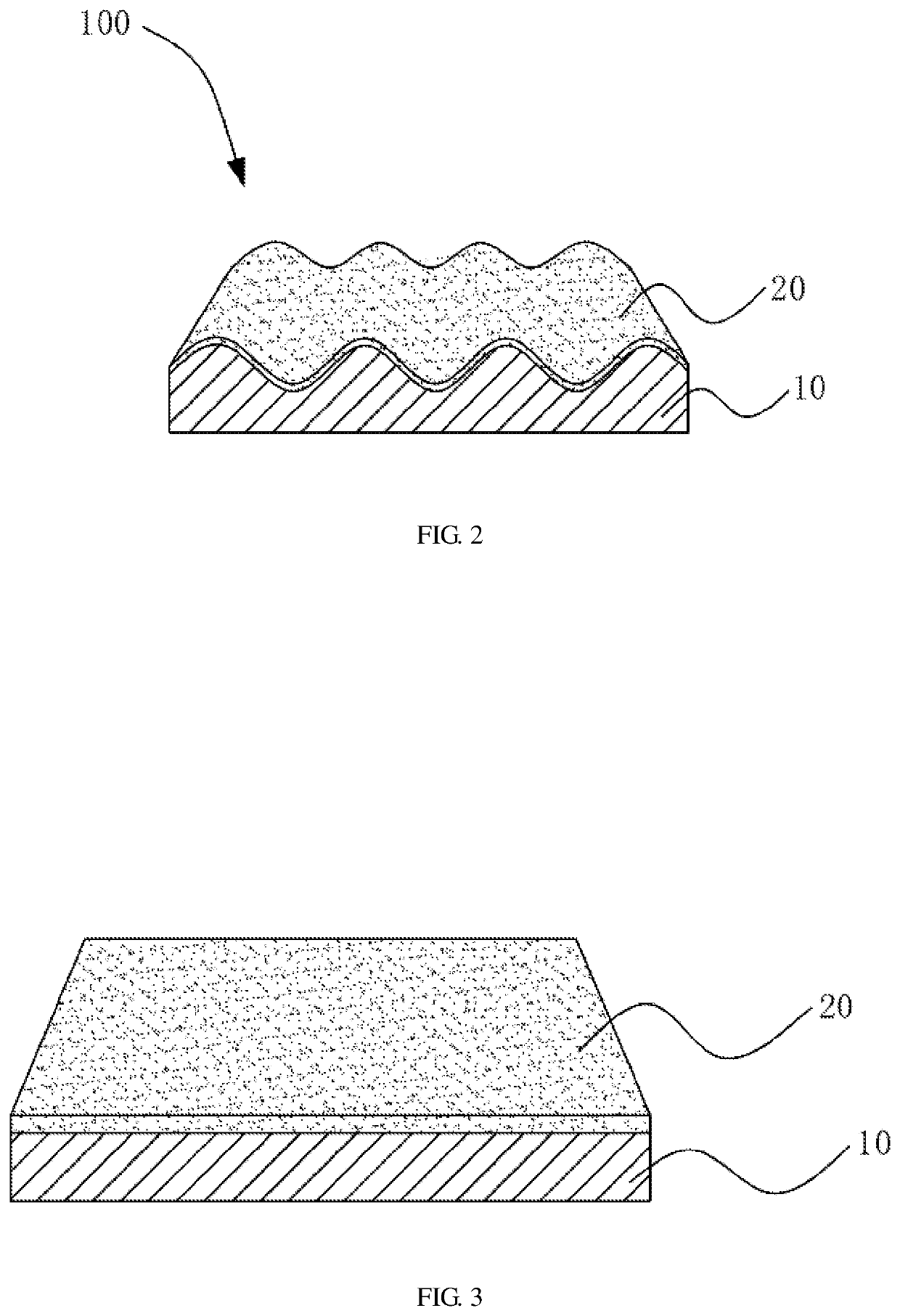
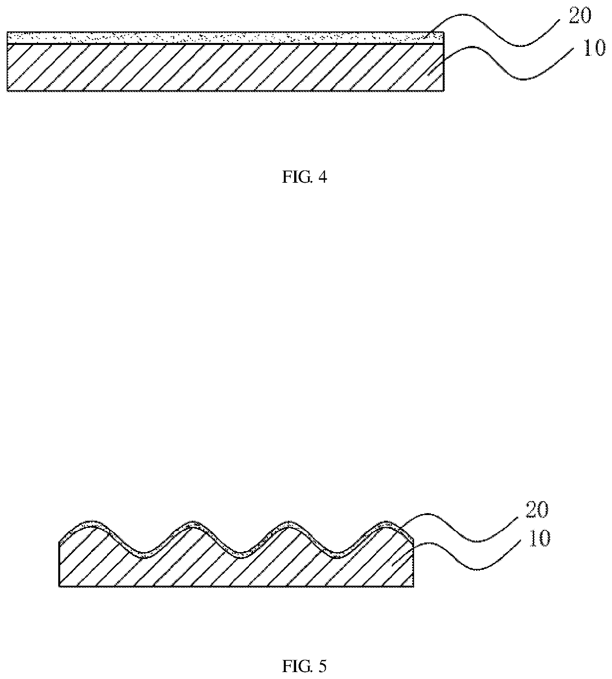
[0046]FIG. 2 illustrates a flexible conductive film 100 according to a first embodiment of the present disclosure. The flexible conductive film 100 includes a bottom film 10 and a conductive layer which is disposed on the bottom film 10. The conductive layer 20 and one side of the bottom film 10 near the conductive layer 20 are both wavy.

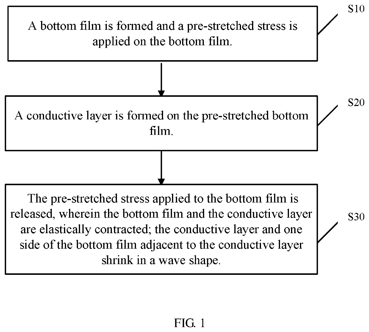
[0047]In FIG. 1, a method of producing the flexible conductive film 100 includes Block S10, Block S20, and Block S30.

[0048]At Block S10, a bottom film 10 is produced and a pre-stretched stress is applied on the bottom film 10.

[0049]Please refer to FIG. 3 and FIG. 4. At first, a bisamino-dimethylsiloxane film serves as the bottom film 10. Next, the transparency of the bottom film 10 is adjusted by pre-stretched stress. So the transparency of the bottom film 10 reaches a set value, and the transparency of the bottom film 10 is controlled within a range of 55% to 88%. When the stretch ratio of the bottom film 10 is 50%, the transparency of the bottom f...

embodiment 2

[0058]In FIG. 6, a flexible conductive film further includes a protective layer 30 disposed on the conductive layer 20. The protective layer 30 covers the conductive layer 20.

[0059]In the present embodiment, a flexible protective layer is added on the basis of the producing method produced by the first embodiment. The flexible transparent material is formed to protect the upper and lower surfaces of the conductive layer 20.

[0060]Followed by Block S30, a step of producing another isamino-polydimethylsiloxane film identical to bottom film 10 is conducted. The isamino-polydimethylsiloxane film is laminated on the conductive layer 20 by molding to form a protective layer 30.

[0061]Similarly, the protective layer 30 with cracks can react with the meta-tribenzaldehyde at room temperature to complete self-healing and crack recovery.

[0062]The flexible conductive film in the present embodiment has two layers of flexible transparent material for protection, which can improve the stability of P...

embodiment 3

[0063]The structure of a flexible conductive film in a third embodiment is the same as the structure of the flexible conductive film in the first embodiment. The method of producing the flexible conductive film of the present embodiment includes Block S10, Block S20, and Block S30.

[0064]At Block S10, a bottom film is produced and a pre-stretched stress is applied on the bottom film.

[0065]A bisamino-dimethylsiloxane film serves as the bottom film. The transparency of the bottom film is adjusted by pre-stretched stress. The transparency of polyurethane elastomers is higher. Different types of polyurethane elastomers is chosen according to the transparency requirements of the bottom film.

[0066]At Block S20, a conductive layer is formed on the pre-stretched bottom film.

[0067]At first, the silver nanowire is transferred onto the pre-stretched bottom film to form a first conductive layer. Afterwards, a graphene oxide is produced by hummers method and a film is formed on the bottom film by...


PUM

PropertyMeasurementUnit
transparencyaaaaaaaaaa

Abstract

A method of producing a flexible conductive film includes: producing a bottom film and applying a pre-stretched stress on the bottom film; forming a conductive layer on the pre-stretched bottom film; and releasing the pre-stretched stress applied to the bottom film wherein the bottom film and the conductive layer are elastically contracted; the conductive layer and one side of the bottom film adjacent to the conductive layer shrink in a wave shape. The method of producing the flexible conductive film provided by the present disclosure can improve the flexibility and the stability of the conductive layer while the conductive layer is being used, thereby improving the service life of the flexible conductive film.

Description

BACKGROUND1. Field of the Disclosure[0001]The present disclosure relates to the field of optics, and more particularly, to a flexible conductive film, a method for producing the flexible conductive film, and a display panel.2. Description of the Related Art[0002]A flexible transparent conductive film has been widely adopted in the field of photovoltaic devices such as liquid crystal displays, touch panels, organic light emitting diodes, and solar cells in recent years owing to features such as electrical conductivity, light transmittance, and bending resistance. Common transparent conductive films are indium tin oxide (ITO) films, metal mesh film, Nano silver wire film and the like.[0003]The technology of the ITO film is mature but the raw material cost of the ITO film is high, the conductivity of the ITO film is limited, and the ITO film is not resistant to bending. The price of the material for a metal mesh film is low and the metal mesh film is resistant to electromagnetic interf...

Claims


Application Information

Patent Timeline
Patent Type & Authority Applications(United States)
IPC IPC(8): B32B27/08H01B1/02C09D5/24C09D165/00B32B27/28B32B3/30B32B37/16
CPCB32B27/08H01B1/02C09D5/24C09D165/00B32B27/283B32B2383/00B32B37/16B32B2255/10B32B2255/26B32B2255/205B32B2457/20B32B3/30H01B13/0026H01B13/0009H01B5/14G06F3/0412G06F2203/04102G06F2203/04103C08G61/126C08G2261/1424C08G2261/3223C08G2261/794C08G2261/91C08G2261/95H01B1/127H01B1/128B32B2250/24B32B27/40B32B2255/28B32B2307/412B32B2307/546B32B2255/20B32B3/085B32B2307/202B32B2274/00Y02E10/549H10K71/60H10K77/111
Inventor LI, YINGLIU, WEIPING
Owner TCL CHINA STAR OPTOELECTRONICS TECH CO LTD
Why Eureka
Try Eureka