Packaging substrate and semiconductor device comprising same

a technology of packaging substrate and semiconductor device, which is applied in the direction of semiconductor device, semiconductor device details, electrical apparatus, etc., can solve the problems of difficult mounting of high-performance and high-frequency semiconductor elements thereon, distinct limitation to the reduction of wiring pitch, and inability to support the entire packaging technology. , to achieve the effect of simplifying the treatment process of an insulating layer, improving electrical properties, and relatively easy mass production

Active Publication Date: 2022-02-17
ABSOLICS INC
View PDF0 Cites 3 Cited by
  • Summary
  • Abstract
  • Description
  • Claims
  • Application Information

AI Technical Summary

Benefits of technology

[0039]Packaging substrate and semiconductor device comprising same of the embodiment can significantly improve electrical properties such as a signal transmission rate by connecting the semiconductor element and a motherboard to be closer to each other so that electrical signals are transmitted through as short a path as possible.
[0040]Also, since a glass substrate applied as a core of substrate is an insulator itself, there is a lower possibility of generating parasitic element compared to a conventional silicon core, and thus it is possible to simplify a process of treatment for an insulating layer and it is also applicable to a high-speed circuit.
[0041]In addition, unlike silicon being manufactured in the form of a round wafer shape, the glass substrate is manufactured in the form of a large panel, and thus mass production is relatively easy and economic efficiency can be further improved.
[0042]Furthermore, by disposing the elements such as a transistor inside the packaging substrate, transmitted electrical signals can be transmitted through a shorter path, so it is possible to have excellent performance with a thinner substrate.
[0043]Besides, it is possible to fix a cavity element in a more accurate position by a supporting unit inside a cavity unit, and workability may be more improved.

Problems solved by technology

Semiconductor technology has been developed in various forms such as line width of a nanometer unit, which is smaller than a micrometer unit, 10 million or more cells, high-speed operation, and much heat dissipation, but technology of packaging it completely is not being supported yet.
In the case of a ceramic substrate such as Si substrate, it is not easy to mount a high-performance and high-frequency semiconductor element thereon due to a high resistance or high dielectric constant.
In the case of a resin substrate, it is possible to mount a high-performance and high-frequency semiconductor element thereon, but there is a distinct limitation to the reduction of pitches of wirings.

Method used


Image

  • Packaging substrate and semiconductor device comprising same
  • Packaging substrate and semiconductor device comprising same
  • Packaging substrate and semiconductor device comprising same

Examples


Embodiment Construction

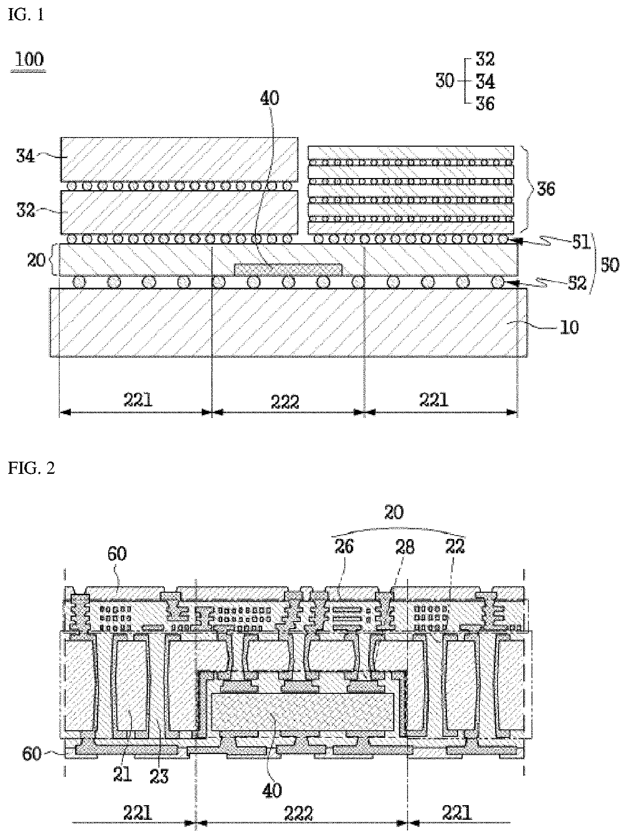
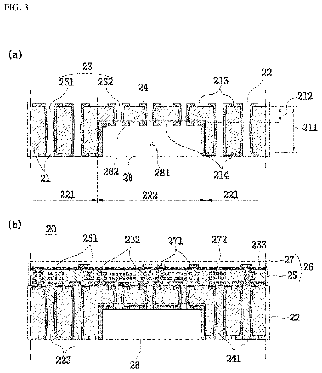
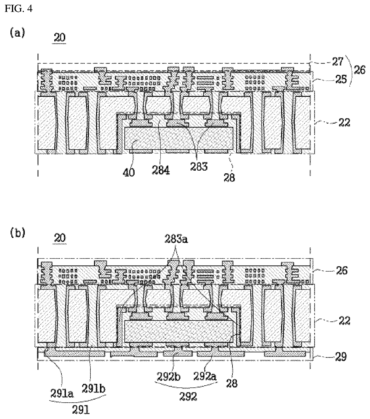
[0059]Hereinafter, examples will be described in detail with reference to the accompanying drawings so that they can be easily practiced by those skilled in the art to which the embodiment pertains. However, the embodiment may be embodied in many different forms and is not to be construed as being limited to the embodiments set forth herein. Like reference numerals designate like elements throughout the specification.

[0060]Throughout the present specification, the phrase “combination(s) thereof” included in a Markush-type expression denotes one or more mixtures or combinations selected from the group consisting of components stated in the Markush-type expression, that is, denotes that one or more components selected from the group consisting of the components are included.

[0061]Throughout the present specification, terms such as “first,”“second,”“A,” or “B” are used to distinguish the same terms from each other. The singular forms “a,”“an,” and “the” include the plural form unless t...


PUM

PropertyMeasurementUnit
thicknessaaaaaaaaaa
thicknessaaaaaaaaaa
thicknessaaaaaaaaaa

Abstract

The embodiment relates to a packaging substrate and a semiconductor device, comprising an element unit comprising a semiconductor element; and a packaging substrate electrically connected to the element unit; and it applies a glass substrate as a core of the packaging substrate, thereby can significantly improve electrical properties such as a signal transmission rate by connecting the semiconductor element and a motherboard to be closer to each other so that electrical signals are transmitted through as short a path as possible. Therefore, it can significantly improve electrical properties such a signal transmission rate, substantially prevent generating of parasitic element, and simplify a process of treatment for an insulating layer, and thus provides a packaging substrate applicable to a high-speed circuit.

Description

CROSS-REFERENCE TO RELATED APPLICATION[0001]This application claims priority to U.S. Provisional Patent Application No. 62 / 816,984, filed on Mar. 12, 2019, US Provisional Patent Application No. 62 / 817,003, filed on Mar. 12, 2019, U.S. Provisional Patent Application No. 62 / 817,027, filed on Mar. 12, 2019, U.S. Provisional Patent Application No. 62 / 825,216, filed on Mar. 28, 2019, U.S. Provisional Patent Application No. 62 / 826,122, filed on Mar. 29, 2019, and U.S. Provisional Patent Application No. 62 / 826,144, filed on Mar. 29, 2019, and all the benefits accruing therefrom under the priority, the content of which in their entireties are herein incorporated by reference.FIELD[0002]The embodiments relate to packaging substrate and semiconductor device comprising same.RELATED ART[0003]In the manufacturing of electronic components, the implementation of a circuit on a semiconductor wafer is referred to as a Front-End Process (FE), and the assembly of a wafer such that it can be actually u...

Claims


Application Information

Patent Timeline
Patent Type & Authority Applications(United States)
IPC IPC(8): H01L23/498
CPCH01L23/49838H01L23/49822H01L23/49827H01L23/49894H01L23/485H01L23/481H01L23/525H01L23/367H01L23/5386H01L23/50H01L23/13H01L23/5389H01L21/4857H01L23/15H01L2224/18H01L2224/73259H01L24/19
Inventor KIM, SUNGJINRHO, YOUNGHOKIM, JINCHEOLJANG, BYUNGKYU
Owner ABSOLICS INC
Why Eureka
Try Eureka