Electrical device and semiconductor apparatus including the same
- Summary
- Abstract
- Description
- Claims
- Application Information
AI Technical Summary
Benefits of technology
Problems solved by technology
Method used
Image
Examples
embodiment 1
[0151]A lower electrode is formed by a DC sputter or an ALD method.
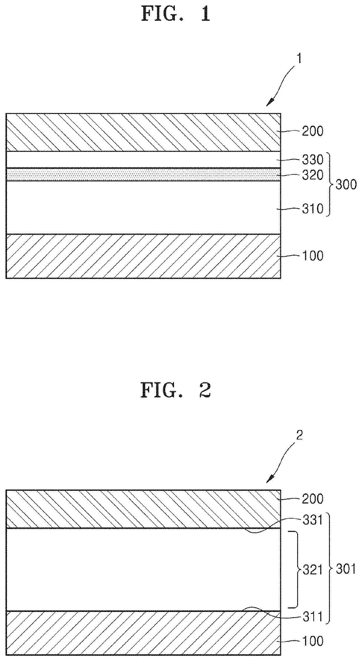
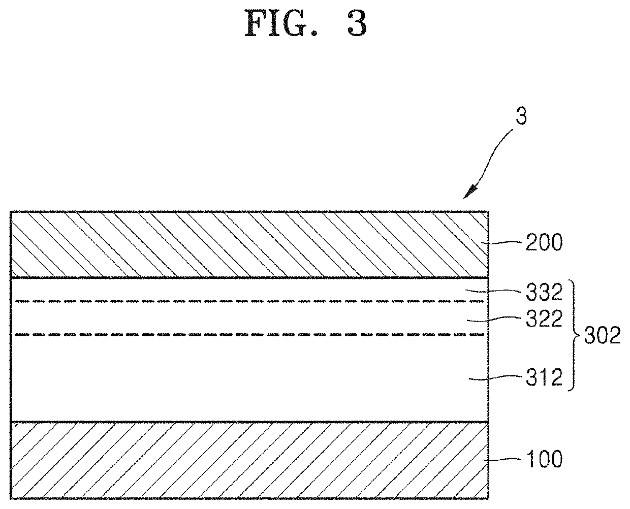
[0152]A dielectric layer is formed on the lower electrode through the ALD method. For example, after forming a first metal oxide layer including ZrO2, a third metal oxide layer including Zr, Al, and B is formed on the first metal oxide layer, and a second metal oxide layer including ZrO2 is formed on the third metal oxide layer. Consequently, the dielectric layer may have a concentration gradation of a boron content of an inner area being greater than boron contents of an upper surface and a lower surface. Furthermore, the amounts of a Zr precursor, an Al precursor, and a B precursor are adjusted during the forming of the dielectric layer such that a content ratio of a B element to an Al element in the third metal oxide layer is 1.0, a content ratio of the B element to a total of metal elements in the third metal oxide layer is 5.0 at %, or a content ratio of the B element to a total of metal elements in the dielectr...
embodiments 2 and 3
[0155]A capacitor is manufactured in the same method as the method of embodiment 1, except that a content ratio between metal elements in the third metal oxide layer and / or a content ratio between metal elements in the dielectric is adjusted, during the forming of the third metal oxide layer, by changing the amounts of the Zr precursor, the Al precursor, and the B precursor as depicted in Table 1.
embodiments 4 and 5
[0162]A capacitor is manufactured in the same method as that of embodiment 1, except that, by adjusting the thicknesses of the first metal oxide layer and the second metal oxide layer, the third metal oxide layer is located at a position of 40% or more of the total thickness of the dielectric layer from the lower electrode (embodiment 4), or at a position of less than 40% of the total thickness of the dielectric layer from the lower electrode (embodiment 5). Consequently, in the dielectric layer of embodiment 4, B may have the maximum concentration at a position at 40% or more of the thickness of the dielectric layer, as measured from the lower electrode, and in the dielectric layer of embodiment 5, B may have the maximum concentration at a position away from the lower electrode by less than 40% of the thickness of the dielectric layer.
[0163]Electrical Property Evaluation 2
[0164]A capacitance by applying 1.0 V to the capacitors of embodiments 4 and 5 and a leakage current value when...
PUM
 Abstract
Description
Claims
Application Information


