Method of making a plurality of high density logic elements with advanced CMOS device layout

a logic element and high density technology, applied in the field of microelectronic devices, can solve the problems of greater challenges in scaling efforts and substantially more difficult application to random logic designs, and achieve the effect of greater precision

Pending Publication Date: 2022-03-31
TOKYO ELECTRON LTD
View PDF5 Cites 2 Cited by
  • Summary
  • Abstract
  • Description
  • Claims
  • Application Information

AI Technical Summary

Benefits of technology

[0007]A stack of dielectric / metal / dielectric is used to make precision gate electrodes that can be scaled to small channel lengths and is self-aligned to the channel. Aspects of the present disclosure enable efficient formation of aligned 3D metal stacks and routing. A multiple threshold voltage, Vt, stack is enabled herein because metal is deposited so each transistor can have an optimum work function. Advanced 3D CMOS metals can withstand high temperatures and may be used prior to epitaxial growth. Gate electrode metal is self-aligned to the channel regions at any distance above the silicon substrate. The process flow can be used for any type of transistor geometry. Embodiments herein are compatible with all transistor types with unique gate electrode formation. More efficient metal gate electrode processing with greater precision is enabled by techniques herein.
[0008]In a first embodiment, a method of microfabrication is describe, the method comprising forming a layer stack on a substrate, the layer stack having a metal layer of a first metal positioned between a first dielectric layer and a second dielectric layer and a first capping layer on the second dielectric layer; forming openings through the layer stack until uncovering the underlying substrate material; epitaxially growing vertical channel structures in the openings for channels of transistors having current flow perpendicular to a working surface of the substrate; and masking the substrate and etching the layer stack leaving sidewall structures of the layer stack on the vertical channel structures, sidewall structures of the first metal forming a gate contact of a field effect transistor.

Problems solved by technology

Scaling efforts have greatly increased the number of transistors per unit area in 2D circuits, yet scaling efforts are running into greater challenges as scaling enters single digit nanometer semiconductor device fabrication nodes.
Although device stacking has been successfully demonstrated and implemented by the flash memory industry with the adoption of 3D NAND, application to random logic designs is substantially more difficult.

Method used


Image

  • Method of making a plurality of high density logic elements with advanced CMOS device layout
  • Method of making a plurality of high density logic elements with advanced CMOS device layout
  • Method of making a plurality of high density logic elements with advanced CMOS device layout

Examples


Embodiment Construction

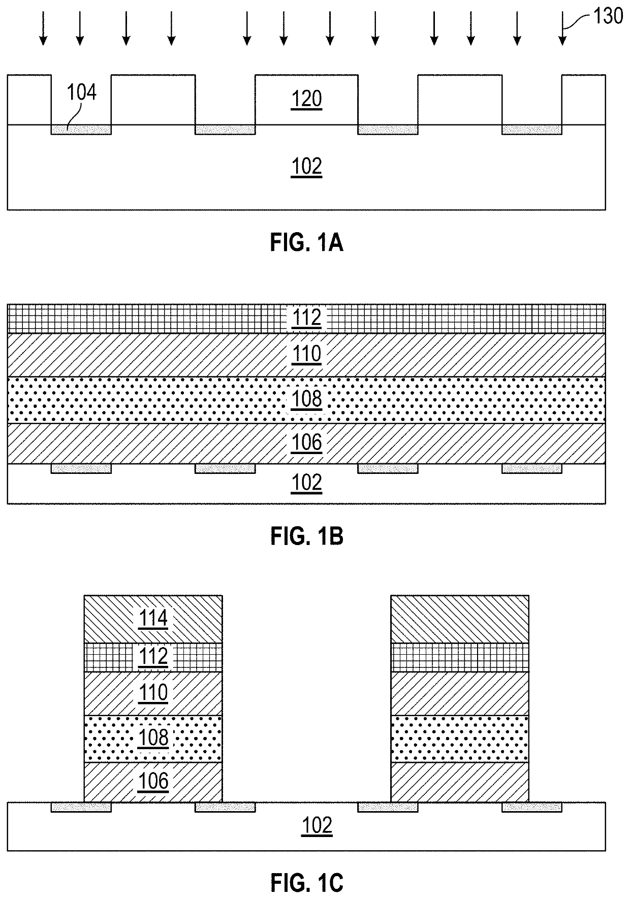
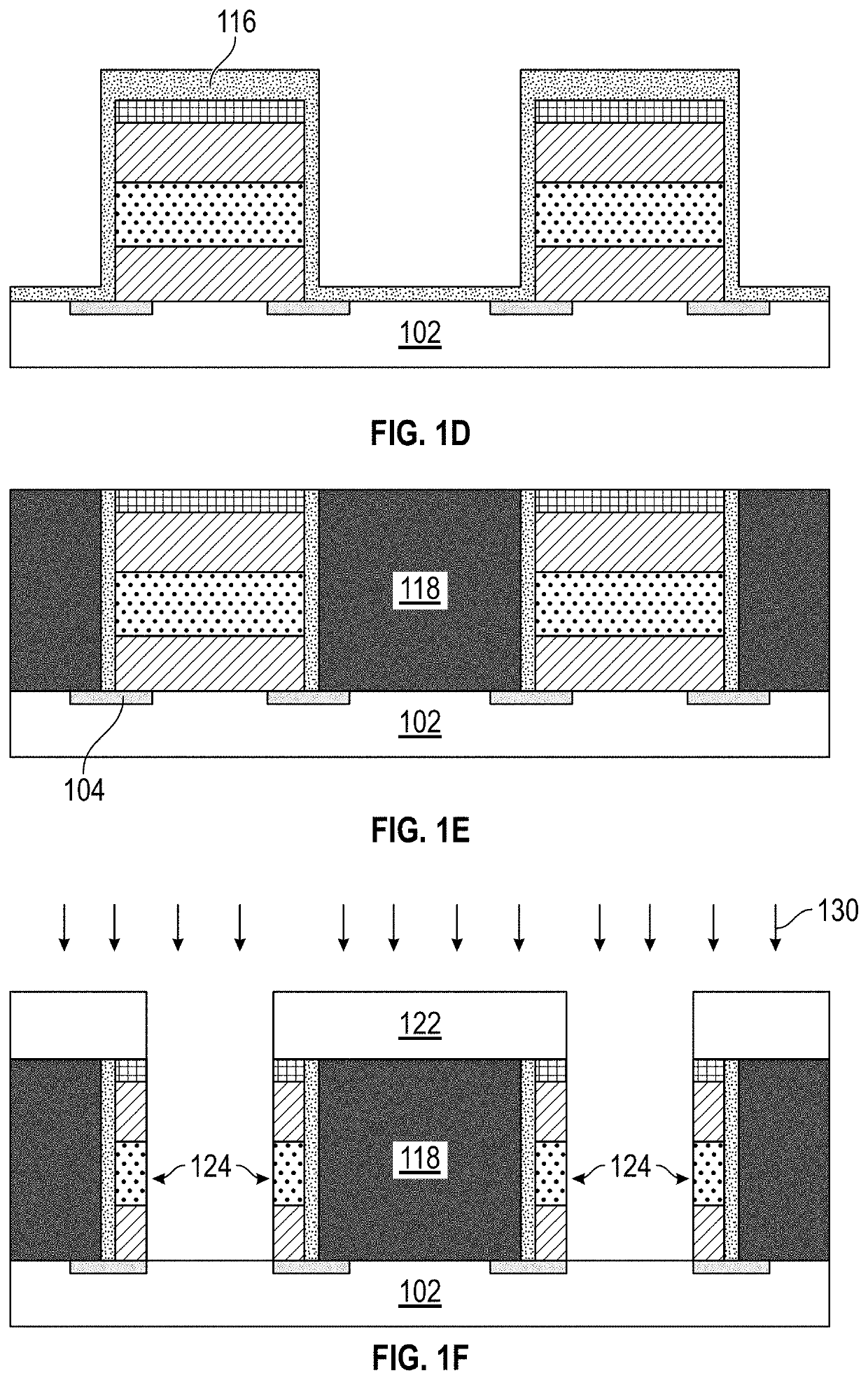
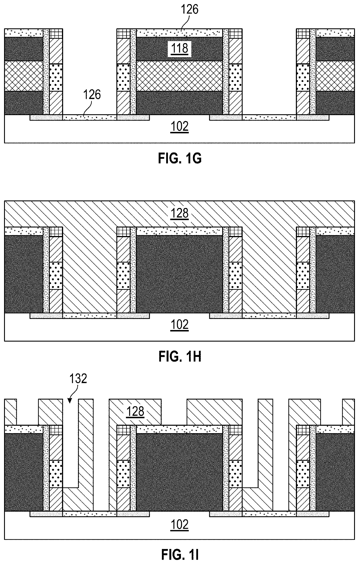
[0051]The following disclosure provides many different embodiments, or examples, for implementing different features of the provided subject matter. Specific examples of components and arrangements are described below to simplify the present disclosure. These are, of course, merely examples and are not intended to be limiting. For example, the formation of a first feature over or on a second feature in the description that follows may include embodiments in which the first and second features are formed in direct contact, and may also include embodiments in which additional features may be formed between the first and second features, such that the first and second features may not be in direct contact. In addition, the present disclosure may repeat reference numerals and / or letters in the various examples. This repetition is for the purpose of simplicity and clarity and does not in itself dictate a relationship between the various embodiments and / or configurations discussed. Furthe...


PUM

PropertyMeasurementUnit
current flowaaaaaaaaaa
P-type semiconductoraaaaaaaaaa
densityaaaaaaaaaa

Abstract

Aspects of the present disclosure provide a 3D semiconductor apparatus and a method for fabricating the same. The 3D semiconductor apparatus can include a first semiconductor device including sidewall structures of a first gate metal sandwiched by dielectric layers, a first epitaxially grown channel surrounded by the sidewall structures; a second semiconductor device formed on the same substrate adjacent to the first semiconductor device that includes sidewall structures of a second gate metal sandwiched by dielectric layers, a second epitaxially grown channel surrounded by the sidewall structures; a salicide layer formed between the first and second semiconductor devices and metallization contacting each of the S/D regions and the gate regions. The 3D semiconductor apparatus may include a P+ epitaxially grown channel formed on the same substrate adjacent to an N+ epitaxially grown channel, the P+ epitaxially grown channel separated from N+ epitaxially grown channel by a diffusion break.

Description

CROSS REFERENCE TO RELATED APPLICATIONS[0001]The present application claims the benefit of U.S. Prov. Ser. No. 63 / 085,627 entitled “Method For Pattern Reduction Using A Staircase Spacer”, filed on Sep. 30, 2020, incorporated herein by reference in its entirety.BACKGROUNDField of the Invention[0002]This disclosure relates to microelectronic devices including semiconductor devices, transistors, and integrated circuits, including methods of microfabrication.Description of the Related Art[0003]The background description provided herein is for the purpose of generally presenting the context of the disclosure. Work of the presently named inventors, to the extent the work is described in this background section, as well as aspects of the description that may not otherwise qualify as prior art at the time of filing, are neither expressly nor impliedly admitted as prior art against the present disclosure.[0004]In the manufacture of a semiconductor device, for example, especially on the micro...

Claims


Application Information

Patent Timeline
Patent Type & Authority Applications(United States)
IPC IPC(8): H01L29/66H01L29/40H01L21/8238H01L27/088H01L27/092
CPCH01L29/66568H01L29/401H01L29/665H01L21/823885H01L21/823842H01L21/823892H01L27/088H01L27/092H01L21/823878H01L27/0925H01L21/823814H01L29/7827H01L29/66666H01L21/823487H01L21/823475H01L21/823871
Inventor GARDNER, MARK I.FULFORD, H. JIM
Owner TOKYO ELECTRON LTD
Why Eureka
Try Eureka