Array substrate, fabricating method thereof, and display device
- Summary
- Abstract
- Description
- Claims
- Application Information
AI Technical Summary
Benefits of technology
Problems solved by technology
Method used
Image

Examples
embodiment 1
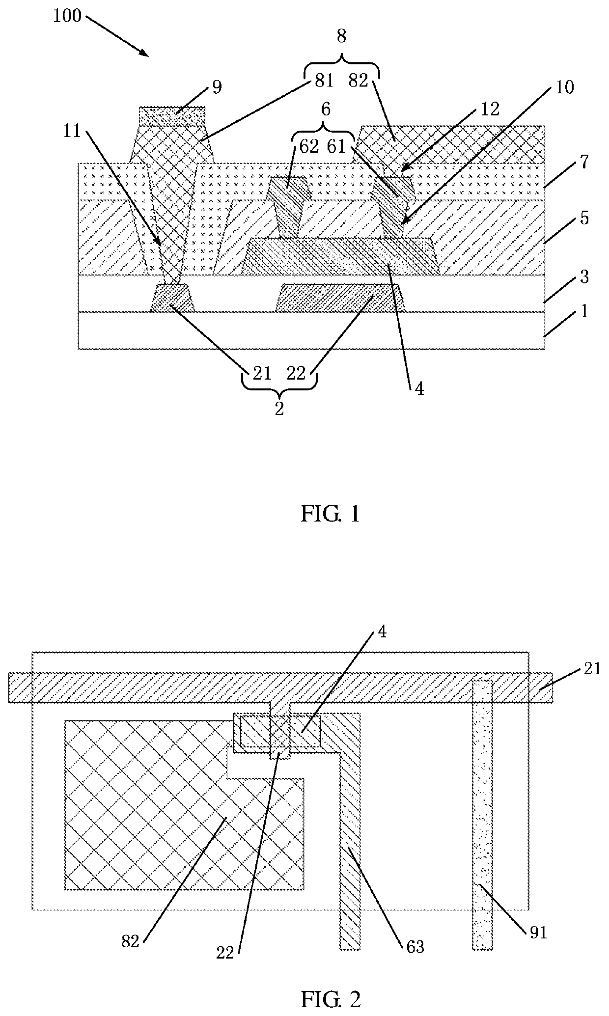
[0030]As shown in FIG. 1 and FIG. 2, an array substrate 100 includes a substrate 1, a first metal layer 2, a gate insulating layer 3, an active layer 4, an etch stop layer 5, a second metal layer 6, a passivation layer 7, a pixel electrode 8, and a third metal layer 9.
[0031]As shown in FIG. 1 and FIG. 2, wherein the first metal layer 2 includes a first scanning signal trace 21 and a gate 22 disposed on the substrate 1. Wherein constituent material of the first metal layer 2 comprises at least one of Mo, Al, Ti, or Cu. The first metal layer 2 thus produced has good electrical conductivity.
[0032]As shown in FIG. 1 and FIG. 2, the gate insulating layer 3 is disposed on the first metal layer 2. Constituent material of the gate insulating layer 3 comprises at least one of SiO2, SiNx, or Al2O3. The gate insulating layer 3 thus produced has good insulation properties, and can prevent the gate 22 from coming into contact with the active layer 4 thereon very well, thereby avoiding a short ci...
embodiment 2
[0039]The embodiment further provides a method for fabricating the array substrate 100 described in the embodiment 1.
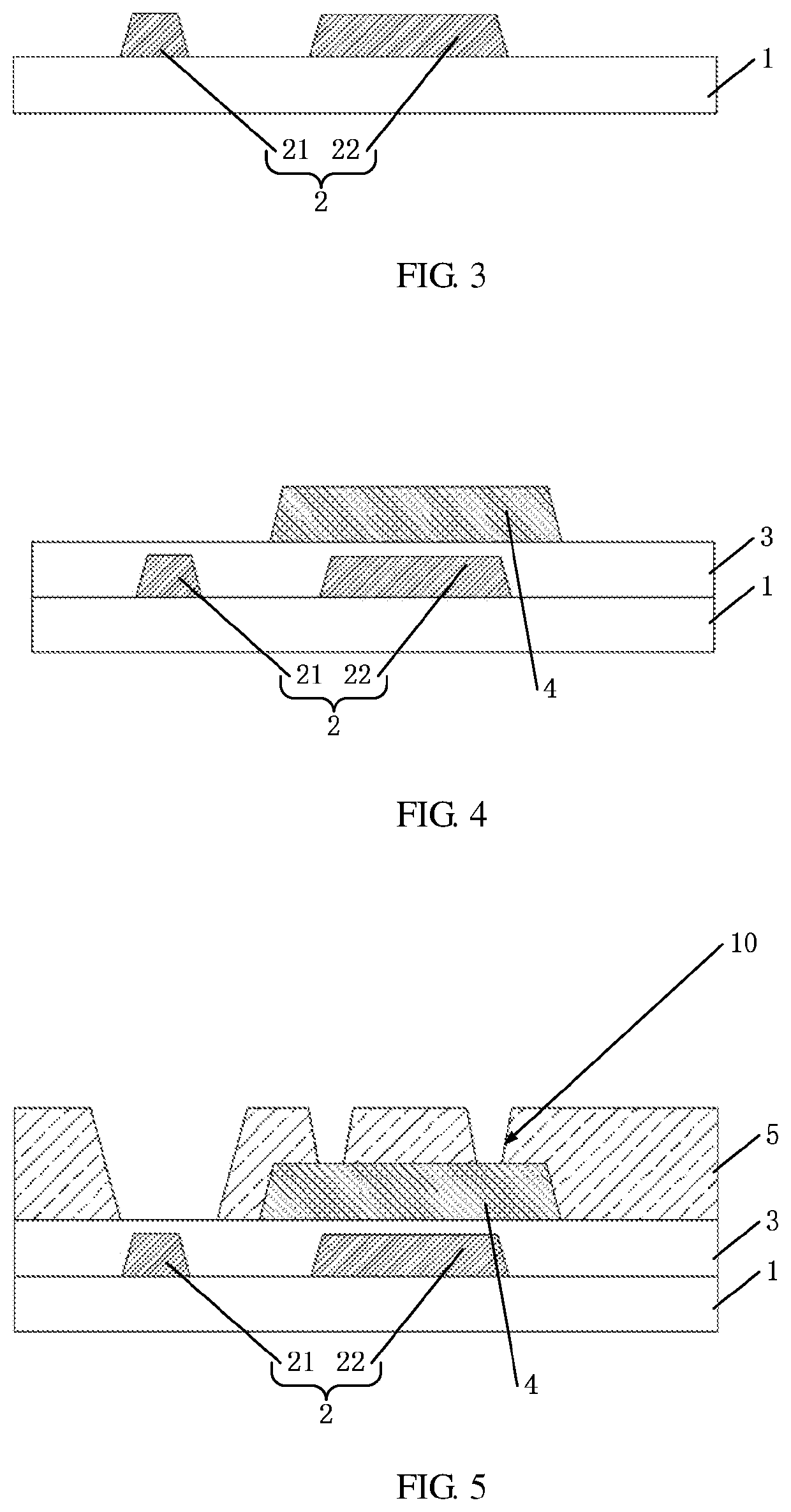
[0040]As shown in FIG. 3, step S1, providing a substrate 1; step S2, forming a first metal layer 2 on the substrate 1 and patterning it to form a first scanning signal line 21 and a gate 22.
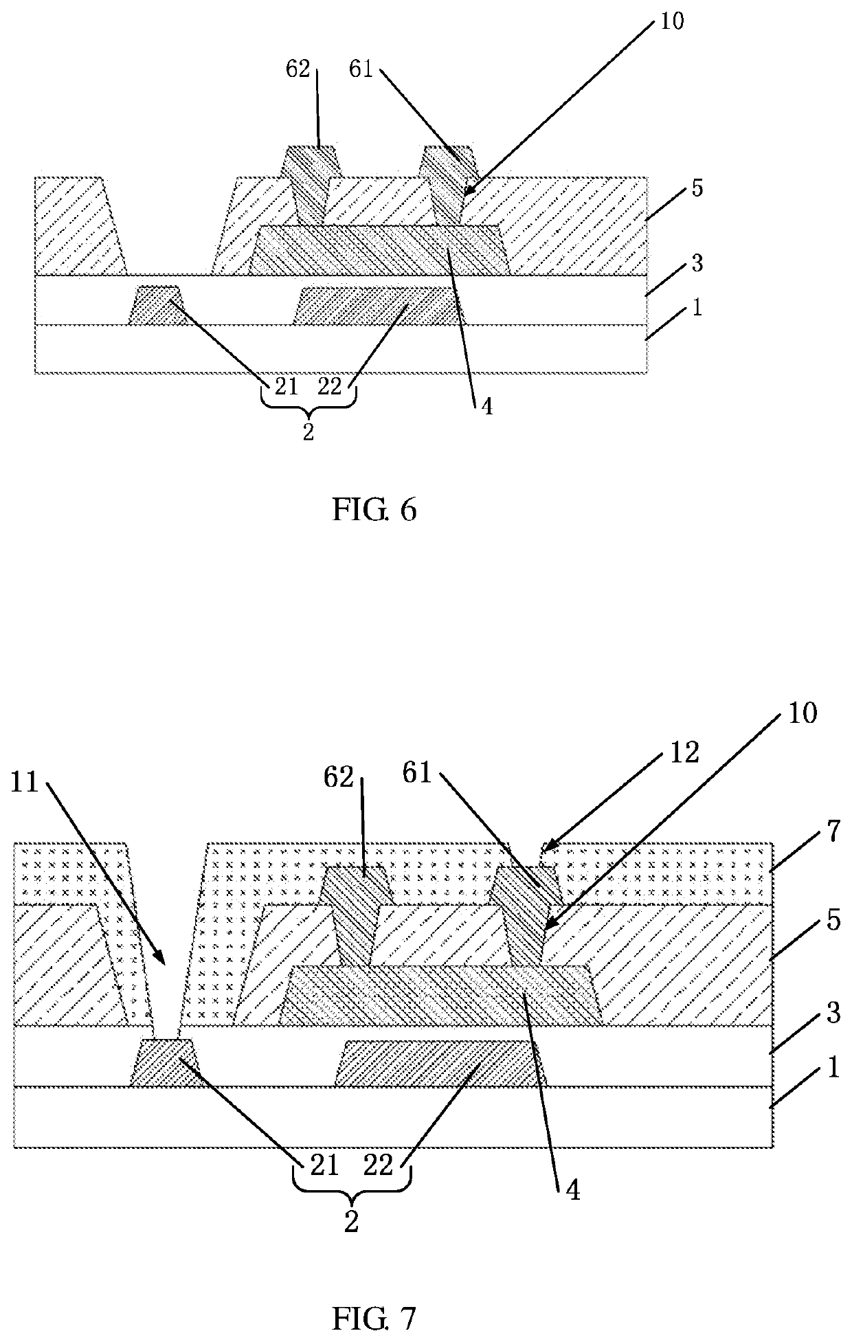
[0041]As shown in FIG. 4, step S3, forming a gate insulating layer 3 on the first metal layer 2; step S4, forming an active layer 4 on the gate insulating layer 3. Wherein the gate insulating layer 3 may be formed by plasma enhanced chemical vapor deposition or sputtering.
[0042]The plasma enhanced chemical vapor deposition is a method in which a gas is excited in a chemical vapor deposition to generate a low temperature plasma and enhance the chemical activity of the reaction material to perform epitaxy. The method has the advantages of low deposition temperature, small influence on the structure and physical properties of the substrate, good film thickness and composition uniformi...
PUM
 Abstract
Description
Claims
Application Information
 - R&D Engineer
- R&D Manager
- IP Professional
- Industry Leading Data Capabilities
- Powerful AI technology
- Patent DNA Extraction
Browse by: Latest US Patents, China's latest patents, Technical Efficacy Thesaurus, Application Domain, Technology Topic.
© 2024 PatSnap. All rights reserved.Legal|Privacy policy|Modern Slavery Act Transparency Statement|Sitemap