

Semiconductor structure and forming method thereof
a technology of semiconductors and forming methods, applied in the direction of semiconductor devices, electrical equipment, transistors, etc., can solve the problem of insufficient surface area of a wafer to fabricate the interconnect lines, and achieve the effect of reducing the resistance of the source/drain plug, reducing the delay of the back-end of line resistance capacitance (rc) and improving the performance of electrical connection
- Summary
- Abstract
- Description
- Claims
- Application Information
AI Technical Summary
Benefits of technology
Problems solved by technology
Method used
Image

Examples
Embodiment Construction
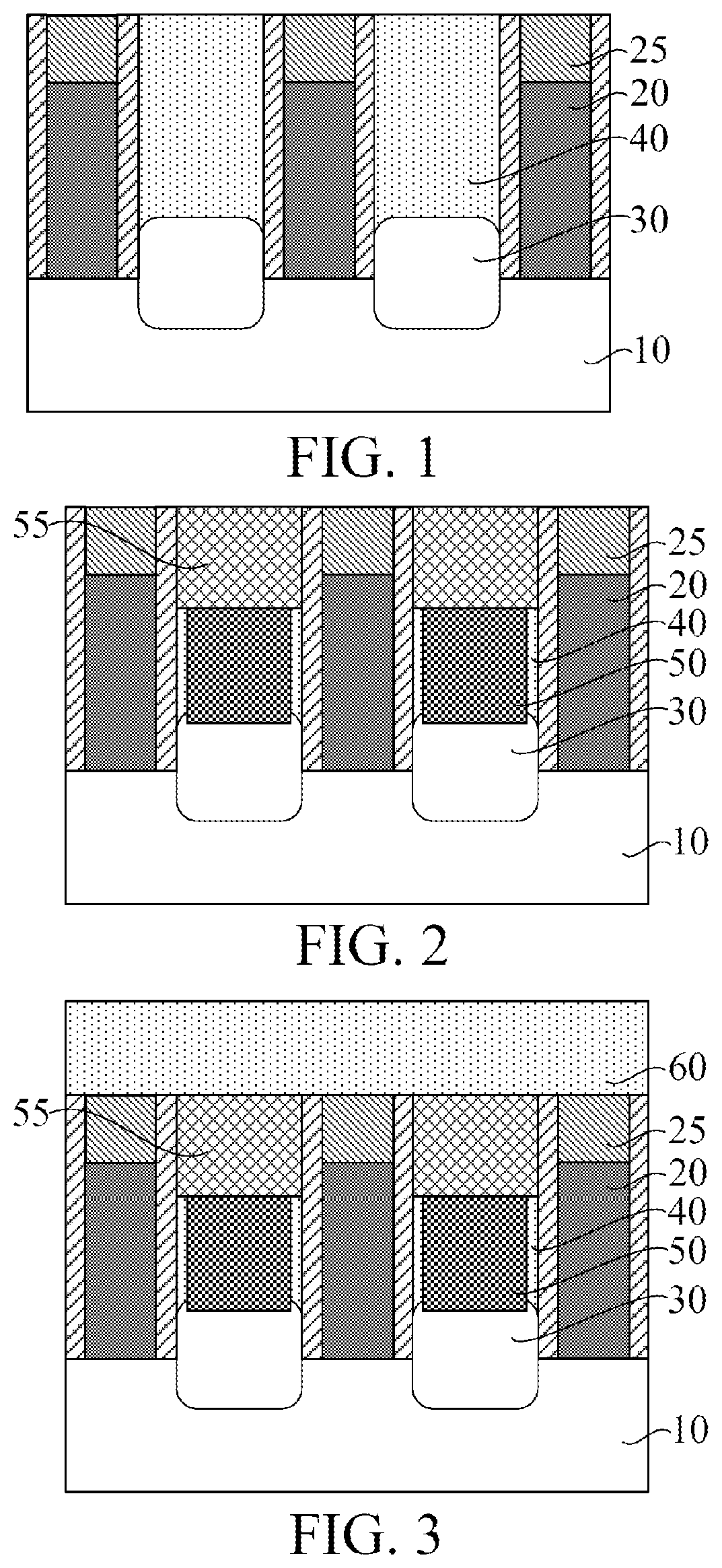
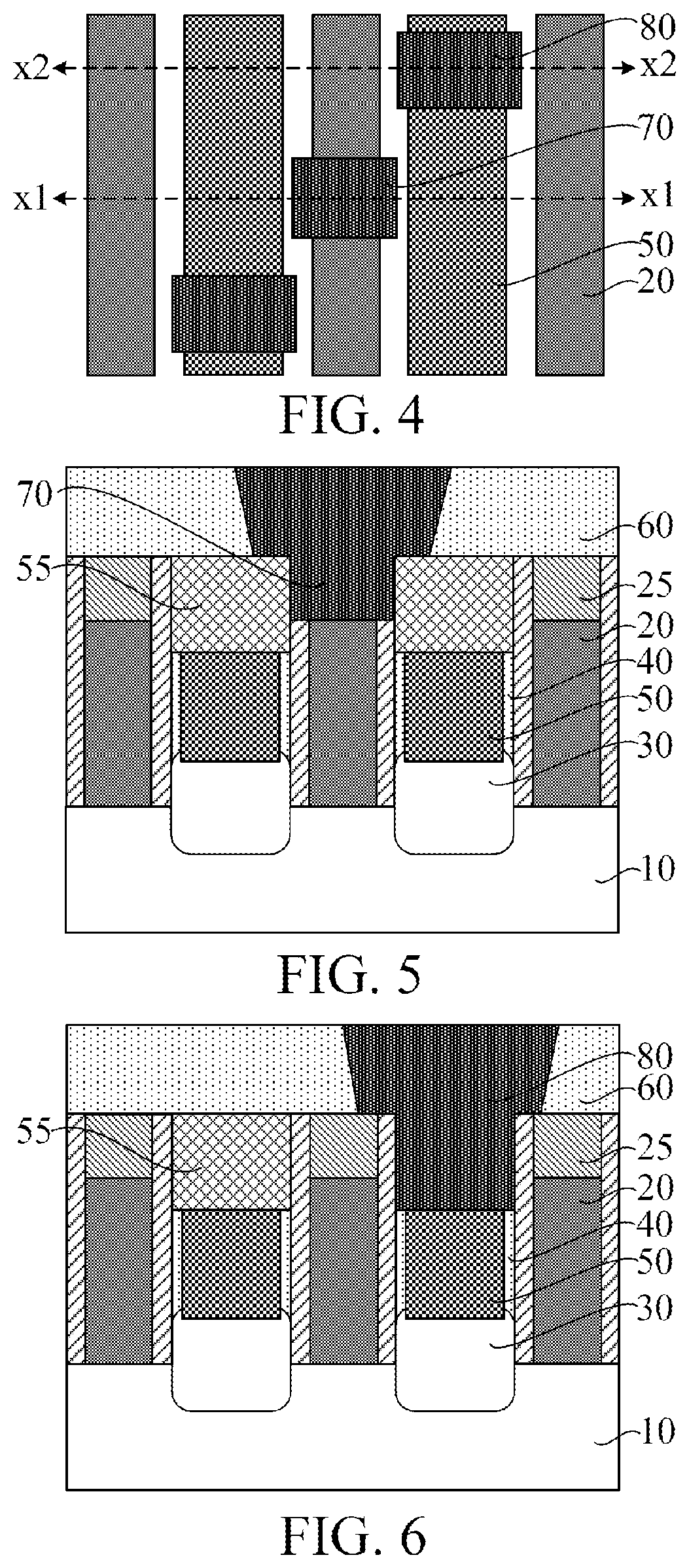
[0017]It can be learned from the related art that, at present, performance of a semiconductor structure needs to be improved. Reasons why the performance of a semiconductor structure needs to be improved are now analyzed in combination with a forming method of a semiconductor structure. FIG. 1 to FIG. 6 are schematic structural diagrams corresponding to steps in a forming method of a semiconductor structure.
[0018]Referring to FIG. 1, a base 10 is provided, gate structures 20 are formed on the base 10, gate cap layers 25 are formed on top surfaces of the gate structures 20, source / drain doped regions 30 are formed in the base 10 on two sides of the gate structures 20, bottom dielectric layers 40 covering the source / drain doped regions 30 are formed on the base 10 on sides of the gate structures 20, and the bottom dielectric layers 40 expose top surfaces of the gate cap layers 25.
[0019]Referring to FIG. 2, source / drain contact layers 50 penetrating the bottom dielectric layers 40 on t...
PUM
| Property | Measurement | Unit |
|---|---|---|
| thicknesses | aaaaa | aaaaa |
| thicknesses | aaaaa | aaaaa |
| aspect ratio | aaaaa | aaaaa |
Abstract
Description
Claims
Application Information