Silicon carbide semiconductor device

Pending Publication Date: 2022-08-11
FUJI ELECTRIC CO LTD
View PDF0 Cites 0 Cited by
  • Summary
  • Abstract
  • Description
  • Claims
  • Application Information

AI Technical Summary

Benefits of technology

[0013]According to an embodiment of the invention, a silicon carbide semiconductor device includes: a silicon carbide semiconductor substrate of a first conductivity type, having a first main surface and a second main surface opposite to each other; a first semiconductor layer of the first conductivity type, provided on the first main surface of the silicon carbide semiconductor substrate, the first semiconductor layer having an impurity concentration lower than an impurity concentration of the silicon carbide semiconductor substrate, the first semiconductor layer having a first surface and a second surface opposite to each other, the second surface facing the silicon carbide semiconductor substrate; a second semiconductor layer of a second conductivity type, provided on the first surface of the first semiconductor layer, the second semiconductor layer having a first surface and a second surface opposite to each other, the second surface of the second semiconductor layer facing the first semiconductor layer; a plurality of first semiconductor regions of the first conductivity type, selectively provided in a surface layer of the second semiconductor layer at the first surface of the second semiconductor layer; a plurality of second semiconductor regions of t

Problems solved by technology

In a MOSFET, as the threshold voltage increases, a possibility of erroneous turning ON due to electromagnetic noise, etc. decreases and thus,

Method used


Image

  • Silicon carbide semiconductor device
  • Silicon carbide semiconductor device
  • Silicon carbide semiconductor device

Examples


first embodiment

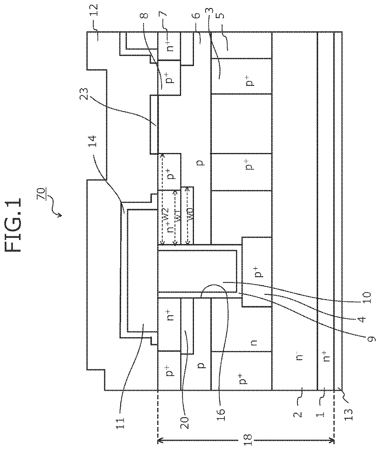
[0036]As depicted in FIG. 1, in the silicon carbide semiconductor device an n−-type silicon carbide epitaxial layer (first semiconductor layer of the first conductivity type) 2 is deposited on a first main surface (front surface), for example, a (0001)-plane (Si-face) of an n+-type silicon carbide substrate (silicon carbide semiconductor substrate of a first conductivity type) 1.

[0037]The n+-type silicon carbide substrate 1 is a silicon carbide single crystal substrate. The n−-type silicon carbide epitaxial layer 2 has an impurity concentration lower than an impurity concentration of the n+-type silicon carbide substrate 1 and, for example, is a low-concentration n-type drift layer. At a first surface of the n−-type silicon carbide epitaxial layer 2, opposite to a second surface thereof facing the n+-type silicon carbide substrate 1, n-type high-concentration regions 5 may be provided in the n−-type silicon carbide epitaxial layer 2. The n-type high-concentration regions 5 constitu...

second embodiment

[0084]As described above, the Schottky-portion p+-type contact regions and the Schottky-portion first p+-type base regions are provided at positions corresponding, in the depth direction, to areas occupied by the Schottky metal. As a result, even in regions below the Schottky metal, the electric field strength may be reduced and application of high electric field to portions of the gate insulating films along the trench bottoms may be prevented.

[0085]In the foregoing, the present invention may be variously modified within a range not departing from the spirit of the invention and in the embodiments described above, for example, dimensions and impurity concentrations of parts, etc. may be variously set according to necessary specifications. Further, in the embodiments, while the first conductivity type is assumed to be an n-type and the second conductivity type is assumed to be a p-type, the present invention is similarly implemented when the first conductivity type is a p-type, and...


PUM


Abstract

A silicon carbide semiconductor device includes a silicon carbide semiconductor substrate of a first conductivity type, a first semiconductor layer of the first conductivity type, a second semiconductor layer of a second conductivity type, first semiconductor regions of the first conductivity type, second semiconductor regions of the second conductivity type, third semiconductor regions of the second conductivity type, provided in the second semiconductor layer at positions facing the first semiconductor regions in a depth direction and having an impurity concentration higher than an impurity concentration of the second semiconductor layer, trenches, gate insulating films, gate electrodes, a first electrode, a second electrode, and third electrodes. The third electrodes form Schottky junctions with the second semiconductor layer and are provided on the surface of portions of the second semiconductor layer free of the third semiconductor regions.

Description

CROSS REFERENCE TO RELATED APPLICATIONS[0001]This application is based upon and claims the benefit of priority of the prior Japanese Patent Application No. 2021-017046, filed on Feb. 5, 2021, the entire contents of which are incorporated herein by reference.BACKGROUND OF THE INVENTION1. Field of the Invention[0002]Embodiments of the invention relate to a silicon carbide semiconductor device.2. Description of the Related Art[0003]Silicon carbide (SiC) is expected to replace silicon (Si) as a next generation semiconductor material. Compared to a conventional semiconductor device in which silicon is used as a semiconductor material, a semiconductor device in which silicon carbide is used as a semiconductor material (hereinafter, silicon carbide semiconductor device) has various advantages as such as enabling use under higher temperature environments (at least 200 degrees C.) and reducing device resistance in an ON state to one of a few hundredths of that of the conventional semiconduct...

Claims


Application Information

Patent Timeline
IPC IPC(8): H01L29/78H01L29/16H01L29/10
CPCH01L29/7806H01L29/7813H01L29/1095H01L29/1608H01L29/872H01L29/0603H01L29/0623H01L29/0878H01L29/66068
Inventor MATSUNAGA, SHINICHIRO
Owner FUJI ELECTRIC CO LTD
Why Eureka
Try Eureka