
Semiconductor Laser and Laser Radar Device Having the Semiconductor Laser

a semiconductor laser and laser radar technology, applied in semiconductor lasers, using reradiation, instruments, etc., can solve the problems of lowering the quality of vehicle control by laser radar devices, such as automatic driving, driving speed control or the like, and unstable optical output of semiconductor lasers

Pending Publication Date: 2022-09-29
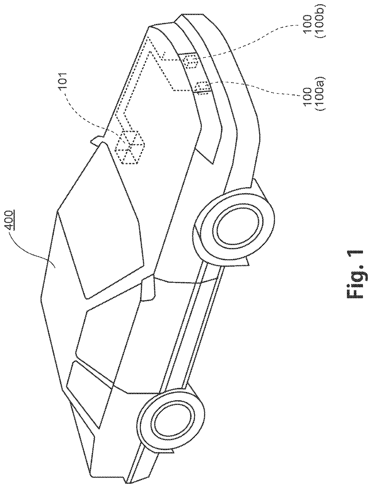
SAE MAGNETICS (HK) LTD
View PDF2 Cites 0 Cited by
  • Summary
  • Abstract
  • Description
  • Claims
  • Application Information

AI Technical Summary

Benefits of technology

The technical effect of this patent is to improve the quality of vehicle control performed by laser radar devices by developing a semiconductor laser that is insensitive to temperature variations. This is achieved by making the semiconductor laser less susceptible to temperature changes, reducing the possibility of mode hopping and ensuring consistent and reliable vehicle control.

Problems solved by technology

Then, it makes optical output of the semiconductor laser unstable.
Therefore, when vehicle control, such as automatic driving, driving speed control or the like, is performed by the laser radar device, control operation of the laser radar device becomes unstable, there is a possibility which the quality of vehicle control by the laser radar device, such as automatic driving, driving speed control or the like, is lowered.

Method used


Image

  • Semiconductor Laser and Laser Radar Device Having the Semiconductor Laser
  • Semiconductor Laser and Laser Radar Device Having the Semiconductor Laser
  • Semiconductor Laser and Laser Radar Device Having the Semiconductor Laser

Examples


first modified example

[0127]Next, the laser diode and the laser radar device, according to the first modified example, will be explained with reference to FIG. 14 to FIG. 18. The laser diode and the laser radar device, according to the first modified example, are respectively different in the active layer of the laser diode, as compared with the above-described laser diode 130 and the laser radar device 100. Namely, in case of the above-described laser diode 130 and the laser radar device 100, the laser diode 130 includes the active layer 145. On the other hand, in case of the laser diode and the laser radar device, according to the first modified example, the laser diode includes an active layer 245, illustrated in FIG. 14 to FIG. 17.

[0128]The active layer 145 includes the five quantum dot layers 161, 162, 163, 164, 165. To the contrary, the active layer 245 includes the five quantum dot layers 171, 172, 173, 174, 175. The active layer 245 has the multi-layered structure which the five quantum dot layer...

second modified example

[0142]Next, the laser diode and the laser radar device, according to the second modified example, will be explained with reference to FIG. 19 to FIG. 23. The laser diode and the laser radar device, according to the second modified example, are respectively different in the active layer of the laser diode, as compared with the above-described laser diode 130 and the laser radar device 100. Namely, in case of the above-described laser diode 130 and the laser radar device 100, the laser diode 130 includes the active layer 145. On the other hand, in case of the laser diode and the laser radar device, according to the second modified example, the laser diode includes an active layer 255, illustrated in FIG. 19 to FIG. 23.

[0143]The above-described active layer 145 includes the five quantum dot layers 161 to 165. To the contrary, the active layer 255 includes the five quantum dot layers 181, 182, 183, 184, 185. The active layer 255 has the multi-layered structure which the five quantum dot...

third modified example

[0156]Next, the laser diode and the laser radar device, according to the third modified example, will be explained with reference to FIG. 24 to FIG. 27. The laser diode and the laser radar device, according to the third modified example, are respectively different in the active layer of the laser diode, as compared with the above-described laser diode 130 and the laser radar device 100. Namely, in case of the above-described laser diode 130 and the laser radar device 100, the laser diode 130 includes the active layer 145. On the other hand, in case of the laser diode and the laser radar device, according to the third modified example, the laser diode includes an active layer 265, illustrated in FIG. 24 to FIG. 27.

[0157]The above-described active layer 145 includes the five quantum dot layers 161 to 165. To the contrary, the active layer 265 includes the five quantum dot layers 191, 192, 193, 194, 195. The active layer 265 has the multi-layered structure which the five quantum dot la...


PUM

PropertyMeasurementUnit
densityaaaaaaaaaa
sizesaaaaaaaaaa
lengthsaaaaaaaaaa

Abstract

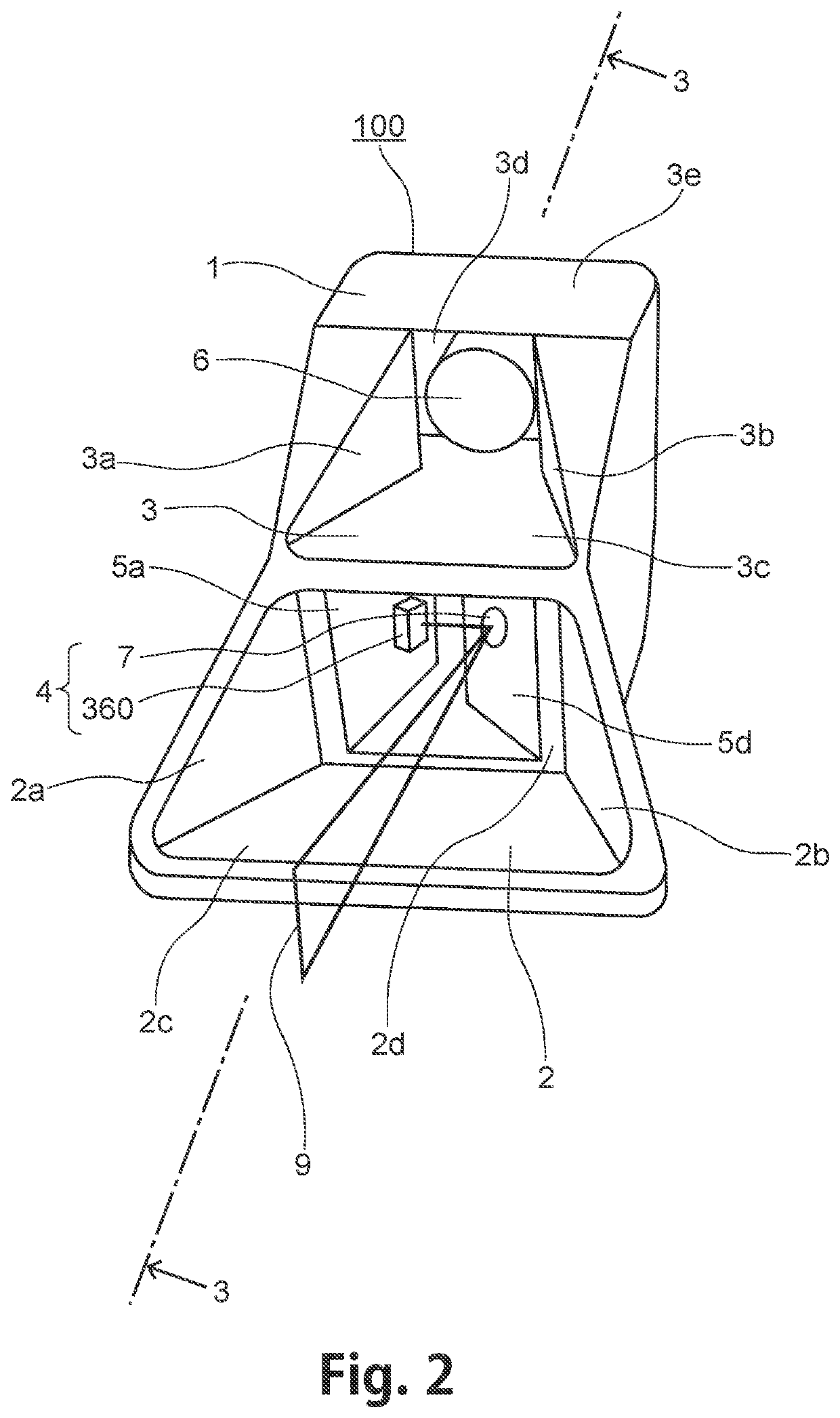
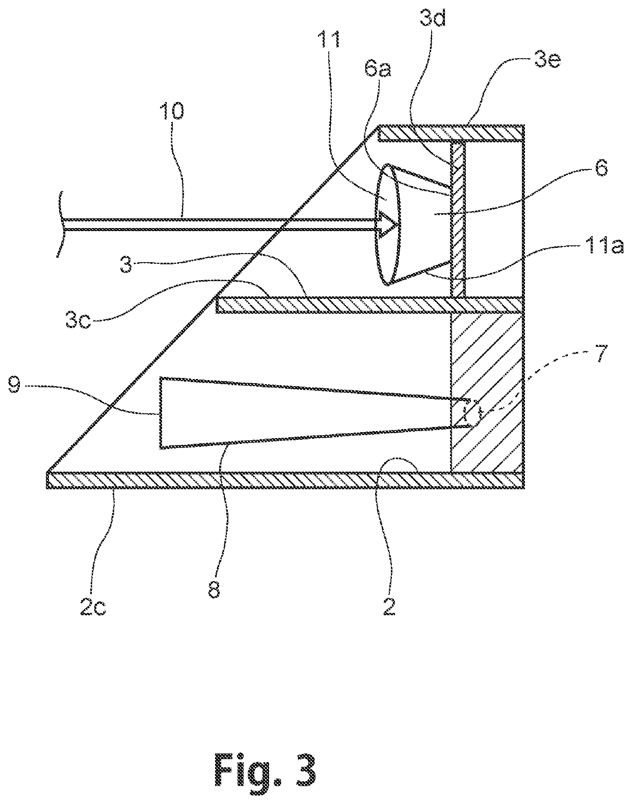
A semiconductor laser includes an active layer which emits laser light and cladding layers being formed so as to sandwich the active layer. The active layer includes a quantum dot layer including a plurality of quantum dots, which respectively confine movements of carriers in the three-dimensional directions. The laser radar device includes a light projection part which projects laser light and a light receiving part which receives reflected light of the laser light. The light projection part includes the semiconductor laser and a scanner which reflects the laser light, emitted from the semiconductor laser, to form a scanning laser light.

Description

BACKGROUNDField of the Invention[0001]The present invention relates to a semiconductor laser and laser radar device having the semiconductor laser.Related Background Art[0002]The semiconductor lasers (referred to also as laser diodes) have been conventionally used in the various fields. For example, the semiconductor lasers have been used in the field of a laser radar. The laser radar is the technology also called LiDAR (Light Detection and Ranging).[0003]The laser radar is the technology that distances to objects, positions and forms of the objects are measured, utilizing laser light emitted from the semiconductor laser.[0004]The laser radar is the technology which is indispensable to vehicle control such as automatic driving, driving speed control or the like. Therefore, devices utilizing the laser radar (laser radar devices) are mounted on the vehicles, and the laser radar devices are utilized for vehicle control such as automatic driving, driving speed control or the like.[0005]...

Claims


Application Information

Patent Timeline
Patent Type & Authority Applications(United States)
IPC IPC(8): H01S5/34H01S5/042H01L33/06G01S17/931
CPCH01S5/3412H01S5/04254H01L33/06G01S17/931H01S5/22H01S5/02335H01S5/0237H01S5/023H01S5/16H01S5/164G01S7/4814
Inventor TAKAYAMA, SEIICHIGAO, KANGHOSOI, RYOFUJII, RYUJI
Owner SAE MAGNETICS (HK) LTD
Learn More