Semiconductor Laser Structure for Higher-Order Mode Suppression

a laser structure and higher-order technology, applied in semiconductor lasers, laser details, electrical equipment, etc., can solve the problems of poor beam quality, leakage current of the shunt, and non-desirable ho lateral modes that begin to lase, so as to increase power and reduce beam quality

Pending Publication Date: 2022-10-27
INTRABAND LLC
View PDF0 Cites 0 Cited by
  • Summary
  • Abstract
  • Description
  • Claims
  • Application Information

AI Technical Summary

Benefits of technology

[0011]The present invention is a semiconductor laser, such as, but not limited to a QCL. The inventive semiconductor laser provides increased power while suppressing non-desirable HO lateral modes that reduce beam quality when compared with quantum cascade lasers known in the prior art. The present invention pertains to a number of commercial applications, not limited to a free-space optical (FSO) communication system in which a semiconductor laser may be used to achieve communication over ranges over 100 km via line-of-sight signaling to a distant receiver.

Problems solved by technology

The semi-insulating layer 12 does not necessarily provide perfect current blocking over the whole area of the laser chip, which in turn can cause a shunt leakage current in the large chip areas outside the buried ridge region.
However, as the core region increases, non-desirable HO lateral modes begin to lase.
These HO modes create poor beam quality that reduces the power that may be delivered to the distant receiver.
Pulsing the laser to send digital information in this case results in a beam that sends “logic 1” in one direction and “logic 0” in a different direction, possibly causing confusion at the receiver.
In addition, changes in beam quality impair the stability of the power.
However, the narrow core region severely restricts the optical power of the laser.

Method used


Image

  • Semiconductor Laser Structure for Higher-Order Mode Suppression
  • Semiconductor Laser Structure for Higher-Order Mode Suppression
  • Semiconductor Laser Structure for Higher-Order Mode Suppression

Examples


Embodiment Construction

[0033]The present invention and the various features and advantageous details thereof are explained more fully with reference to the non-limiting embodiments described in detail in the following description.

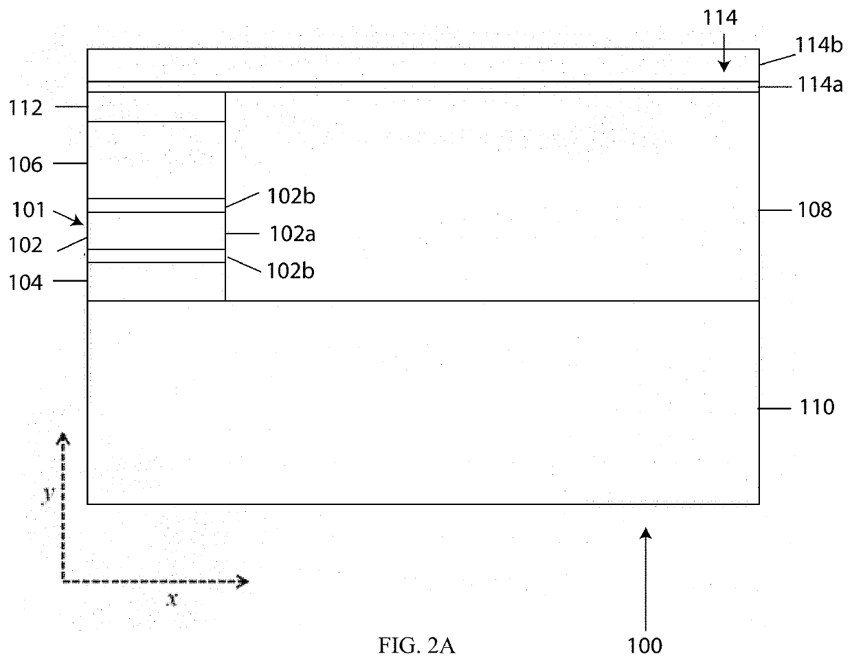
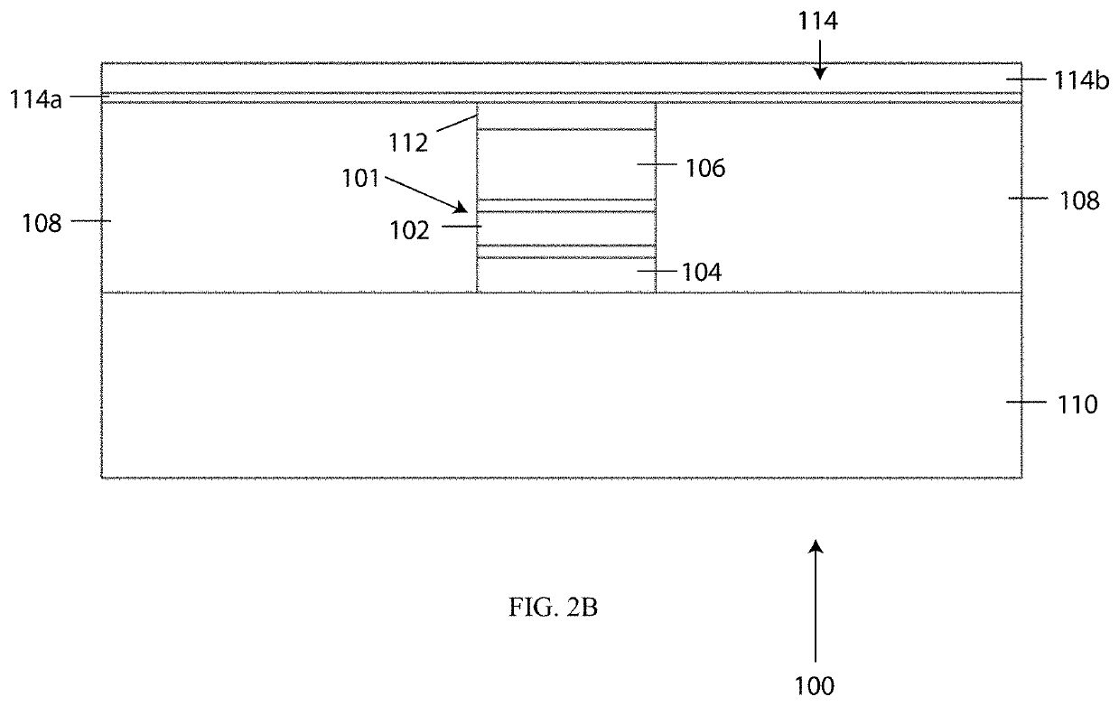
[0034]Referring to FIG. 2A, a structure 100 of a semiconductor laser is shown in accordance with an embodiment of the invention. The structure 100 is intended to support lasing of the fundamental mode at a wavelength of 4.6 μm. The layer thicknesses of the structure 100 of FIG. 2A are not drawn to scale. Further, FIG. 2A only illustrates the right half of the structure 100 (x>0). The structure 100 is symmetric in the x-coordinate. For instance, FIG. 2B represents the complete structure 100 as mirrored about the x-coordinate. The below described doping layers are preferably doped with silicon unless otherwise stated. Further, the level of doping (i.e., 2E16, 2E18, etc.) refers to the doping per cm3.

[0035]As shown in FIG. 2, the structure 100 includes a central ridge 101 including ...


PUM

PropertyMeasurementUnit
widthaaaaaaaaaa
wavelengthaaaaaaaaaa
thicknessaaaaaaaaaa

Abstract

A semiconductor laser including a waveguide having a core, a confinement layer to bury the core, and a metallization layer. The core includes an active core region. The confinement layer surrounds the core and includes a first confinement layer between the core and the semiconductor substrate below the core, a second confinement layer above the core, and a third confinement layer to either or both sides of the core. The metallization layer is located above the confinement layers and include a first metallization layer and a second metallization layer. The first metallization layer is in direct contact with the second confinement layer and the third confinement layer, while the second metallization layer is disposed above the first layer. The first metallization layer is tuned to have a plasmon resonance corresponding to a higher order mode with high loss.

Description

CROSS-REFERENCE TO RELATED APPLICATION[0001]This application claims priority to U.S. Provisional Application No. 63 / 178,302, filed on Apr. 22, 2021, the entire contents of which are hereby expressly incorporated by reference into the present application.REFERENCE TO GOVERNMENT GRANT[0002]This invention was developed with government support under SBIR Contract N689362000070 awarded by the U.S. Navy. The government has certain rights in the invention.BACKGROUND OF THE INVENTION1. Field of the Invention[0003]The present invention relates to a semiconductor laser, such as, but not limited to, a quantum cascade laser (QCL) and a method of manufacturing the lasing structure. The semiconductor laser of the present invention provides increased power while suppressing non-desirable higher-order (HO) lateral modes that reduce beam quality.2. Discussion of the Related Art[0004]A quantum cascade laser (QCL) is a type of semiconductor laser formed by depositing layers of semiconductor material o...

Claims


Application Information

Patent Timeline
Patent Type & Authority Applications(United States)
IPC IPC(8): H01S5/065H01S5/343H01S5/34H01S5/22
CPCH01S5/0653H01S5/34313H01S5/3402H01S5/2206H01S5/3401H01S5/227H01S5/04253H01S5/04252H01S5/2022H01S2301/166H01S5/2224H01S5/0014H01S5/04254
Inventor JACOBS, STEVEN A.MARSLAND, ROBERT A.
Owner INTRABAND LLC
Why Eureka
Try Eureka