Integrated circuit comprising a non-volatile memory of the eeprom type and corresponding manufacturing method

a non-volatile memory, integrated circuit technology, applied in the direction of basic electric elements, electrical apparatus, semiconductor devices, etc., can solve the problems of short channel effect, instabilities and reliability problems, and reduced channel length of state transistors

Pending Publication Date: 2022-11-17
STMICROELECTRONICS (ROUSSET) SAS
View PDF0 Cites 0 Cited by
  • Summary
  • Abstract
  • Description
  • Claims
  • Application Information

AI Technical Summary

Benefits of technology

The patent proposes a method for improving the performance and size of memory cells by preventing the source region from diffusing inside the channel during the implantation process. This is achieved by using a mask to prevent the implantation of the lightly doped region in the source region of the state transistor. The technical effect is that this method reduces the risk of misalignment and ensures a consistent channel length, resulting in a smaller memory cell size.

Problems solved by technology

This can typically result in a reduction in the length of the channel of the state transistor, which generates instabilities and reliability problems.
A channel length which is too short resulting from these variations can cause short channel effects and severe degradations by hot carriers during the programming phases.
The short channel effects are conventionally a physical limitation to the shrinkage of memory cells, in the direction of the length of the channel.
However, the channel length 11 cannot be reduced because of the short channel effects, and the measurement 19 between the edge of the structure SGF10 and a metal contact pillar CNT also cannot be reduced because of a risk of short-circuit with the gates SGF10.

Method used


Image

  • Integrated circuit comprising a non-volatile memory of the eeprom type and corresponding manufacturing method
  • Integrated circuit comprising a non-volatile memory of the eeprom type and corresponding manufacturing method
  • Integrated circuit comprising a non-volatile memory of the eeprom type and corresponding manufacturing method

Examples


Embodiment Construction

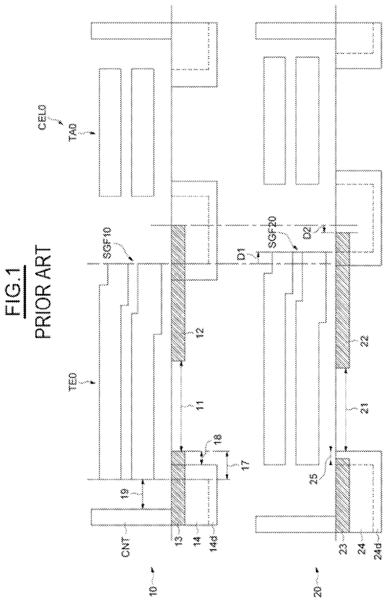
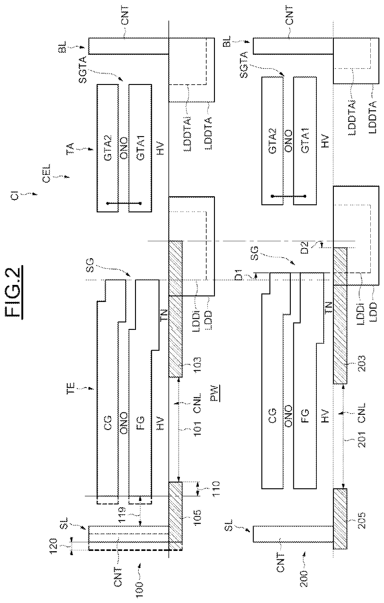
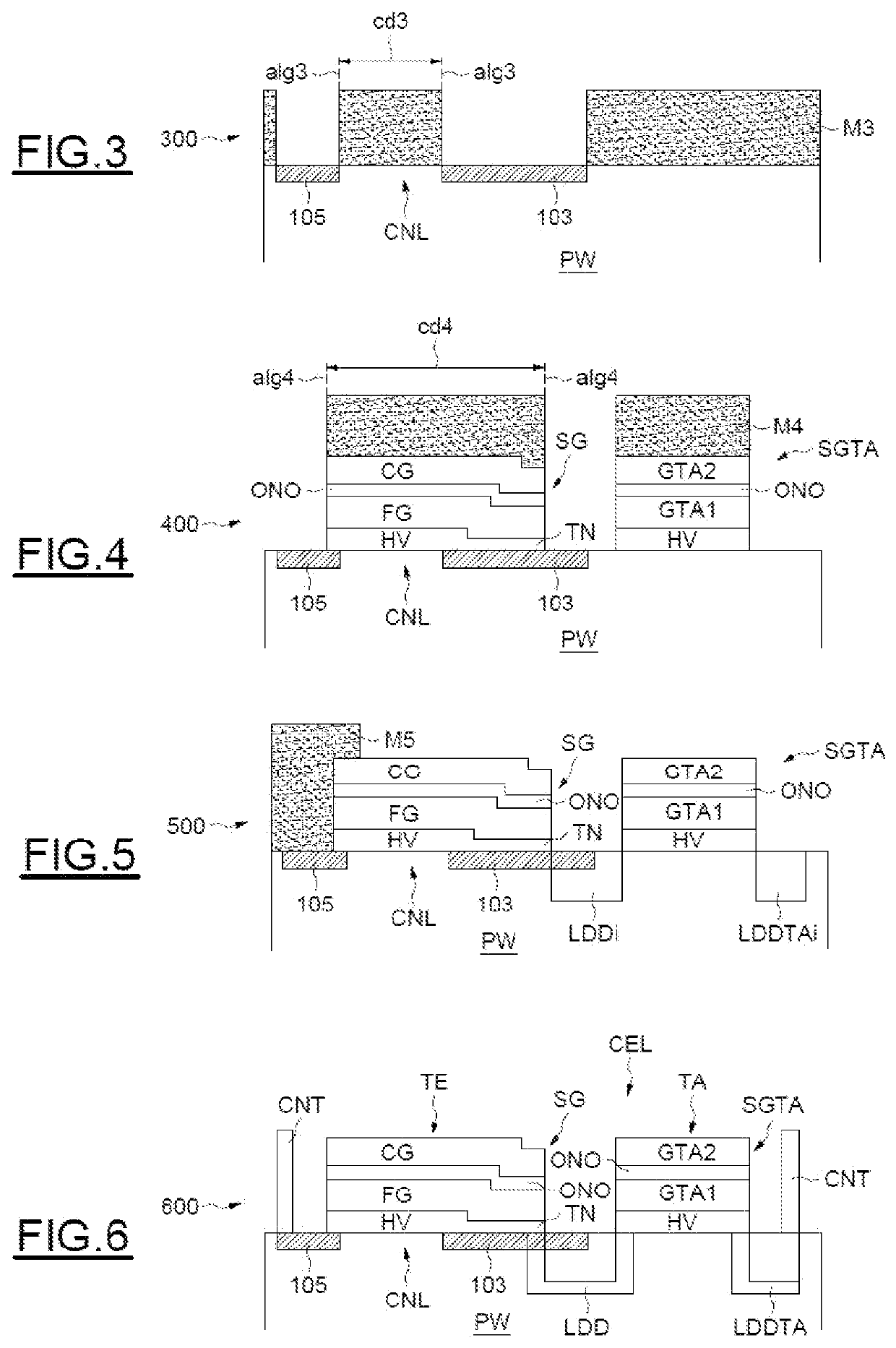
[0053]FIG. 2 illustrates a sectional view of a memory cell CEL belonging to an integrated circuit CI of A non-volatile memory of the electrically erasable and programmable type EEPROM. The EEPROM memory typically includes a memory plane provided with memory cells CEL, which can represent more than 50% of the total size of the integrated circuit CI, and a peripheral control circuit.

[0054]The memory cell CEL is represented in a nominal position 100 and in an “offset” position 200.

[0055]Each memory cell CEL includes a state transistor TE and an access transistor TA in series, made from a semiconductor well PW belonging to a semiconductor substrate of the integrated circuit CI, typically made of P-type doped silicon.

[0056]The state transistor TE is adapted to store binary data and comprises in this regard a gate structure SG comprising a control gate CG and a floating gate FG. The floating gate FG is electrically insulated from the control gate by an inter-gate dielectric layer ONO and ...


PUM

PropertyMeasurementUnit
avalanche voltageaaaaaaaaaa
thickness TNaaaaaaaaaa

Abstract

The integrated circuit of a non-volatile memory of the electrically erasable and programmable type includes memory cells, each memory cell having a state transistor including a gate structure comprising a control gate and a floating gate disposed on a face of a semiconductor well, as well as a source region and a drain region in the semiconductor well. The drain region includes a first capacitive implant region positioned predominantly under the gate structure and a lightly doped region positioned predominantly outside the gate structure. The source region includes a second capacitive implant region positioned predominantly outside the gate structure, the source region not including a lightly doped region.

Description

BACKGROUNDTechnical Field[0001]Embodiments and implementations concern the field of electrically erasable and programmable non-volatile memories “EEPROM” (acronym for “Electrically Erasable and Programmable Read Only Memory”), made on an integrated circuit and the corresponding manufacturing methods.Description of the Related Art[0002]An EEPROM memory is typically composed of a memory plane of memory cells, which are adapted to store data, and a management circuit, in particular adapted to carry out writes and reads in the memory plan.[0003]The EEPROM memory cells typically include a state transistor in series with an access transistor, the state transistor being a floating gate transistor adapted to store a data bit, the access transistor allowing selectively controlling the access to the state transistors belonging to a group of memory cells called memory word.[0004]A constant objective in the field of EEPROM memories is to reduce the surface area of the memory cells. This can typ...

Claims


Application Information

Patent Timeline
Patent Type & Authority Applications(United States)
IPC IPC(8): H01L27/11529H01L27/11524H10B41/41H10B41/35
CPCH01L27/11529H01L27/11524H01L29/42368H01L29/42376H01L29/7883H10B41/35H10B41/41
Inventor TAILLIET, FRANCOISSIMOLA, ROBERTOBOIVIN, PHILIPPE
Owner STMICROELECTRONICS (ROUSSET) SAS
Why Eureka
Try Eureka