Clock distribution load buffer for an integrated circuit

Inactive Publication Date: 2000-01-04
IBM CORP
View PDF11 Cites 40 Cited by
  • Summary
  • Abstract
  • Description
  • Claims
  • Application Information

AI Technical Summary

Benefits of technology

It is another object of the present invention to provide a high speed buffer for enhancing clock signal distribution.
The foregoing objects are achieved as is now described. A system for synchronizing circuit operation within an integrated circuit having a high frequency clock is provided. The system includes an oscillator for providing a clock signal and a transmission line coupled to the oscillator for distributing the clock signal to load buffers. The load buffers provide sub-circuits within the integrated circuit with synchronized clock signals. The load buffers are resonant and convert the capacitive load impedance of receiving circuits into a virtual inductive load. The impedance converter boosts the clock signal transition times to provide improved high frequency circuit synchronization within the integrated circuit.

Problems solved by technology

As clock speeds and the scale of integrated circuits continues to increase, timing difficulties associated with wire lengths have become a vexing problem.
The R-C delay associated with circuit interconnection is prone to process variations across the chip because the product (R-C) depends on the thickness of the conductor and the fabrication of the dielectric layers.
Process variations result in intolerable timing skews in separate geographical areas of the integrated circuit.
The large number of inverts utilized as load buffers causes timing skews due to across chip channel length variations, increased chip area, and constraints in chip layout and planning.
Such low impedances result in large current transients (.about.10 A) during clock signal transitions, and high instantaneous currents create many problems in the power distribution network.

Method used


Image

  • Clock distribution load buffer for an integrated circuit
  • Clock distribution load buffer for an integrated circuit

Examples


Embodiment Construction

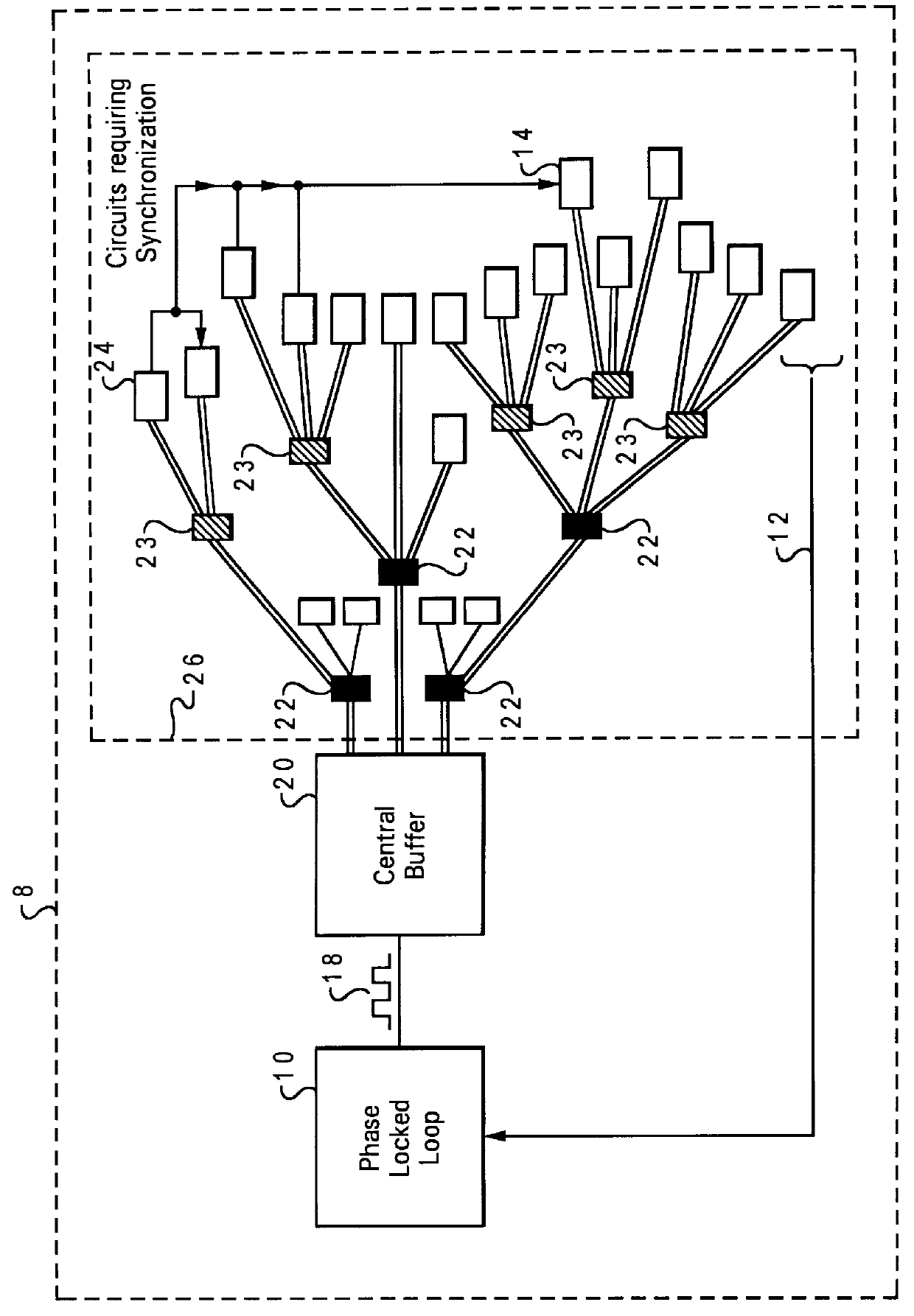
With reference now to the figures and in particular with reference to FIG. 1, there is depicted a clock signal distribution system utilizing a transmission line network 26. Transmission line network 26 conducts clock signal 18 throughout integrated circuit 8.

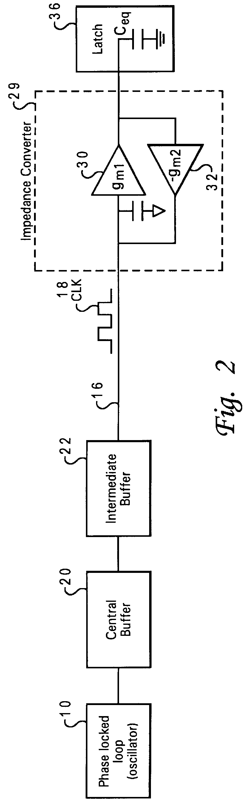
Typically, a precision oscillator, such as a phase locked loop 10, is utilized within integrated circuit 8 to provide a stable clock signal 18 for the synchronization of data transfer. Phase locked loop 10 provides central buffer 20 with clock signal 18. Phase locked loop 10 produces clock signal 18 which has a low level and must be amplified and conditioned by central buffer 20 before distribution to sub-circuits to ensure system integrity.

Phase locked loop 10 receives feedback via sense line 12. Feedback ensures proper precision of clock signal 18 at receiving subcircuits. Many circuits and topologies could provide a precision clock signal for utilization in conjunction with the present invention. Phase locked loop 10 of FIG. ...


PUM


Abstract

A system for synchronizing circuit operation within an integrated circuit having a high frequency clock. The system includes an oscillator for providing a clock signal and a transmission line coupled to the oscillator for distributing the clock signal to load buffers. The load buffers provide sub-circuits within the integrated circuit with synchronized clock signals. The load buffers are resonant and convert the capacitive load impedance of receiving circuits into a virtual inductive load. The impedance converter boosts the clock signal transition times to provide improved high frequency circuit synchronization within the integrated circuit.

Description

1. Technical FieldThe present invention relates in general to clock signal distribution within an integrated circuit and in particular, to a high speed buffer for enhancing clock signal distribution. Still more particularly, the present invention relates to a high speed resonant buffer for providing high speed clock signal distribution within an integrated circuit.2. Description of the Related ArtSynchronization of logic circuits within an integrated circuit is accomplished by distributing a master clock signal to timing critical sub-circuits. The proper operation of an information processing unit, such as a microprocessor, requires that digital data is in the proper state when data is transferred by the clock signal. In all "clocked" systems there is a master clock which synchronizes circuits and controls the transfer of data.Typically, an oscillator within an integrated circuit produces a clock signal and a central buffer amplifies the signal for distribution to digital sub-circui...

Claims


Application Information

Patent Timeline
IPC IPC(8): G06F1/10
CPCG06F1/10
Inventor GHOSHAL, UTTAM SHYAMALINDU
Owner IBM CORP
Why Eureka
Try Eureka