
Test system and test method for liquid crystal display device

a liquid crystal display and test system technology, applied in the direction of measurement devices, electronic circuit testing, instruments, etc., can solve the problems of failure to identify defects, pixel defects for on-point or off-point, and failure to provide results that are very inadequa

Inactive Publication Date: 2000-01-11
AU OPTRONICS CORP
View PDF3 Cites 25 Cited by
  • Summary
  • Abstract
  • Description
  • Claims
  • Application Information

AI Technical Summary

Benefits of technology

It is another object of the present invention to conduct an electric test and an optical test under the same conditions so as to improve test accuracy and test efficiency.

Problems solved by technology

Theoretically, therefore, it can be ascertained that liquid crystal panel defects found by the optical test are the results of problems that occur during the cell forming process, such as dust entering a liquid crystal cell when it is sealed or the occurrence of scratches.
However, when the reason for the failure of a defective panel found by the optical test is analyzed, it is found that the reason the failure occurred is not always dust or scratches, and the cause may be by the electrical characteristics of a pixel capacitor.
It is felt that although originally electric characteristics are detected at the electric test, the reason that such a failure is found during the optical test is that it is caused by a device used for the test, the test method or differences in the testing conditions.
The pixel defect for an ON point or an OFF point that is to be examined at the optical test can be caused by a signal line short circuit, a line break or a pixel capacitor failure, or by the entry of dust or by scratches acquired during the cell forming process.
However, since visually a defect caused by either failure has the same appearance, the cause of the defect can not be identified merely through visual observation.
For this reason, both an electric testing device and an optical testing device must be employed to analyze a failure and to determine its cause, and such an analysis of a failure provides results that are very inadequate.

Method used


Image

  • Test system and test method for liquid crystal display device
  • Test system and test method for liquid crystal display device
  • Test system and test method for liquid crystal display device

Examples


Embodiment Construction

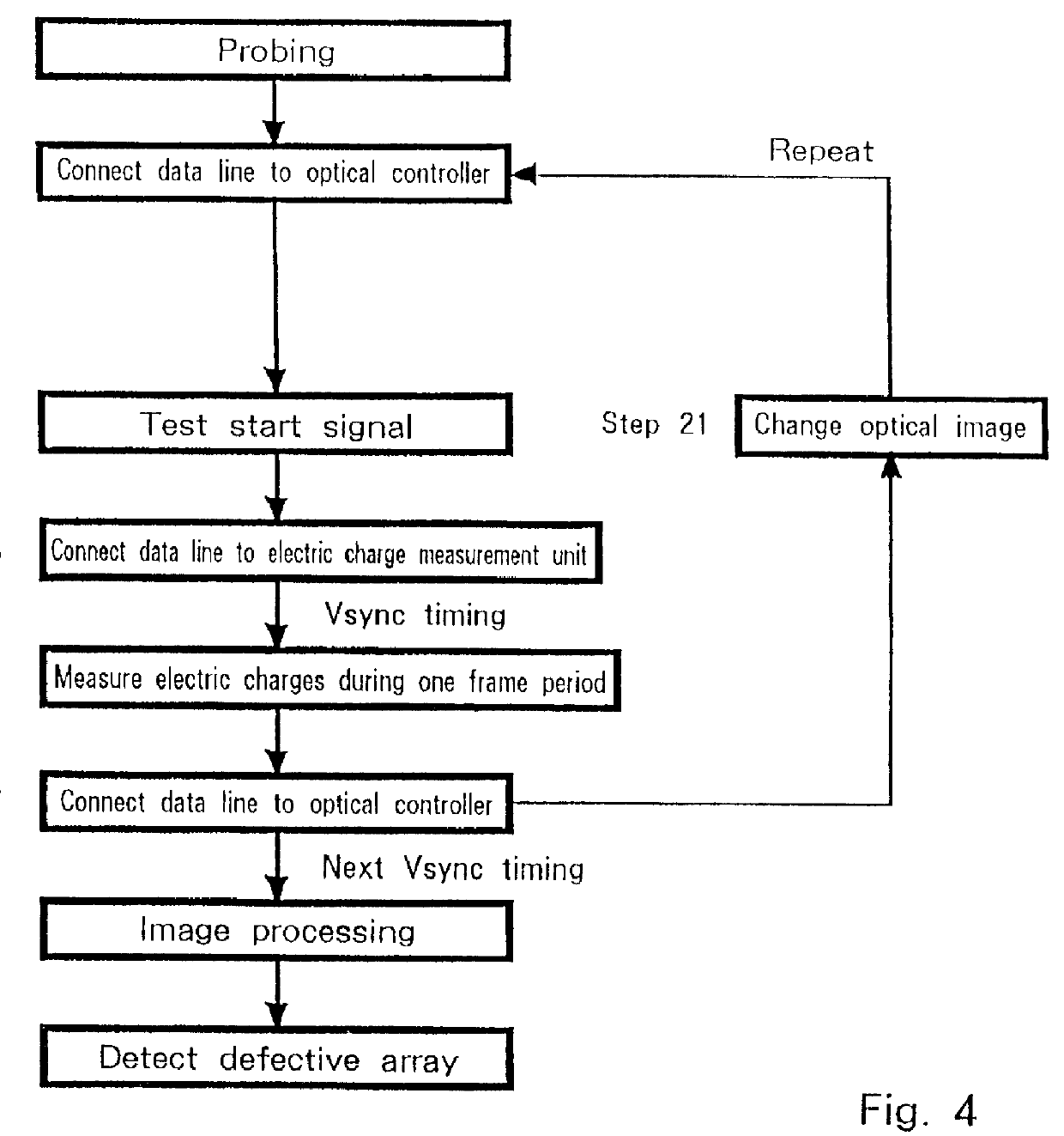
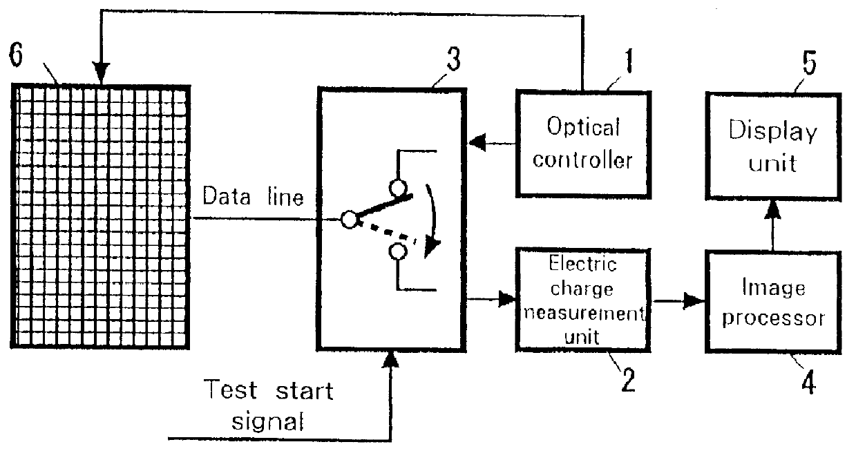
Fig.2 is a block diagram illustrating a test system for a liquid crystal panel according to one embodiment of the present invention. The test system comprises an optical controller 1, serving as signal supply means; an electric charge measurement unit 2; a test switching unit 3; an image processor 4; and a display unit 5. First, a data line of a liquid crystal panel 6 to be tested is connected to the test switching unit 3, and its gate line is connected to the optical controller 1. The test switching unit 3 is so set that the data line is connected to the optical controller 1. The optical controller 1 transmits a control signal to the gate line and the data line of the liquid crystal panel 6, and turns the liquid crystal panel on. That is, electric charges are accumulated in the pixel capacitor of the liquid crystal panel 6. Since the liquid crystal panel 6 is in the ON enabled state when the cell forming process is terminated, it is turned on upon the receipt of the control signal....


PUM

PropertyMeasurementUnit
capacitancesaaaaaaaaaa
electric testaaaaaaaaaa
optical testaaaaaaaaaa

Abstract

The present invention is directed to a new test system by which an electric test and an optical test for a liquid crystal display device, such as a liquid crystal panel, can be performed at the same time and under the same conditions, and to enhancing the test accuracy and the test efficiency. More particularly, the present invention is directed to a test system for a liquid crystal display device comprising: an optical controller 1 for supplying a control signal to a gate line and a data line of a liquid crystal panel 6 that is to be examined; an electric charge measurement unit 2 for measuring pixel capacitances of pixels in one frame of the liquid crystal panel 6; a test switching unit 3 for, in response to a test start signal instructing that the electric test be started, connecting the data line of the liquid crystal panel 6, which has connected to the optical controller 1, to the electric charge measurement unit 2 during a period equivalent to one frame; an image processor 4 for performing image processing for the electric charge value measured by the electric charge measurement unit 2; and a display unit 5 for displaying the resultant image.

Description

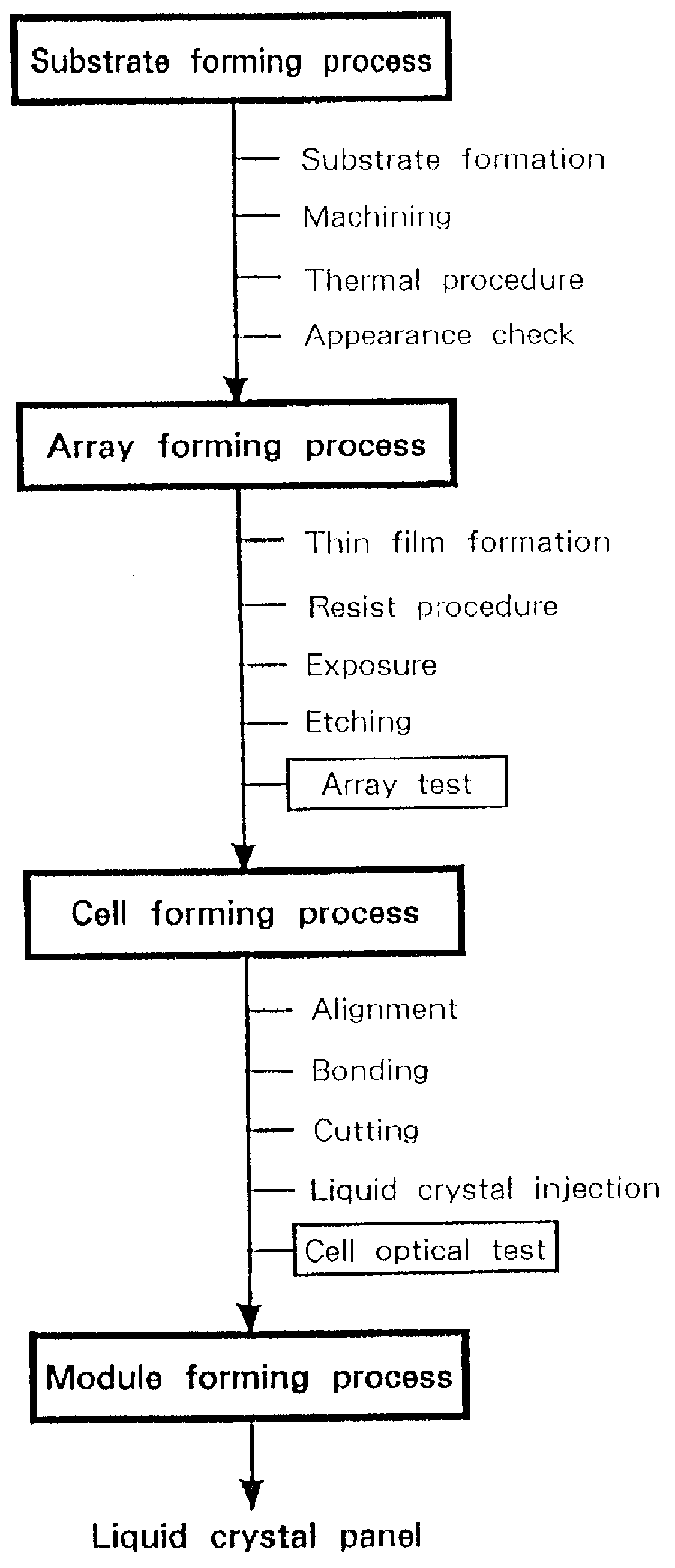
1. Technical FieldThe present invention relates to a test system having both an electric test function and an optical test function for testing a liquid crystal display device, such as a liquid crystal panel, and a test method therefor.2. Prior ArtAs is shown in a flowchart in FIG. 1, a liquid crystal panel is fabricated in a substrate forming process, an array forming process, a cell forming process and a module forming process. Generally, in this fabrication processing series, an electric test, called an array test, is conducted at the final stage of the array forming process, and a cell optical test is conducted at the final stage of the cell forming process. As the electric test in the array forming process, a TFT array test or an open short circuit test is commonly performed. According to the TFT array test, an electric charge writing voltage is applied to a data line and a voltage is applied to a scan line, so that electric charges are written to a pixel capacitor to be tested...

Claims


Application Information

Patent Timeline
Patent Type & Authority Patents(United States)
IPC IPC(8): G09G3/00G02F1/13G01R31/02G01R31/00
CPCG09G3/006G02F1/1309
Inventor TANIGUCHI, YOSHIYUKI
Owner AU OPTRONICS CORP
Learn More