
Method and apparatus for reducing radiated electromagnetic emissions from harmonic frequencies for electronic equipment

a technology of harmonic frequency and electromagnetic emission, applied in the direction of generating/distributing signals, pulse techniques, instruments, etc., can solve the problems of increasing unwanted electromagnetic emissions at various frequencies, excessive electromagnetic emissions from electronic systems may illogically synchronize the operations of nearby electronic systems, and other deleterious effects of electromagnetic radiation have been proved problemati

Inactive Publication Date: 2000-01-11
QUIET SOLUTION
View PDF3 Cites 47 Cited by
  • Summary
  • Abstract
  • Description
  • Claims
  • Application Information

AI Technical Summary

Benefits of technology

is to provide an improved class of devices that is readily available to replace, and compatible in physical fitting and electrical operation to ...

Problems solved by technology

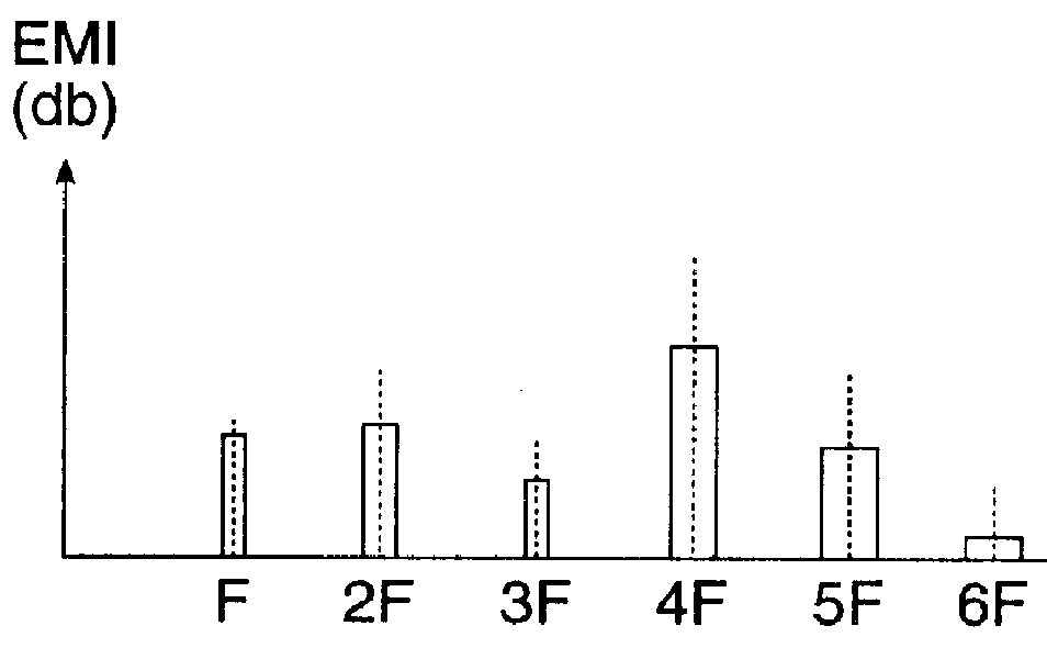
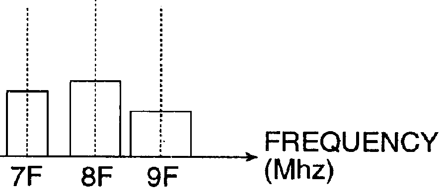
One side effect of the higher clock speeds and additional circuit elements has been increased unwanted electromagnetic emissions at various frequencies, especially at very high frequencies.
It has been known for a long time that excessive electromagnetic emissions from an electronic system may illogically asynchronize operations of nearby electronic systems.
Other deleterious effects of electromagnetic radiation have been proved problematic in many areas.
These measures place a tremendous pressure on manufacturers that design and manufacture electronic systems, all must be certified by the regulations before being released to marketplace.
However, as the frequency of the clocking source gets higher, these methods become less effective and the cost of the shielding increases considerably.
However, none have demonstrated practical solutions to or satisfy current systems.
Most electronic equipment, however, would not work properly if the clock frequency were varied over a wide range.
Both aforementioned methods have failed to address concerns of compatibility with the most widely used oscillating devices such as crystal resonators where there is no dedicated power input to energize the electronics required for those methods to work.
Further these solutions have failed to address concerns of power consumption and physical fitting in aforementioned approaches and examples.

Method used


Image

  • Method and apparatus for reducing radiated electromagnetic emissions from harmonic frequencies for electronic equipment
  • Method and apparatus for reducing radiated electromagnetic emissions from harmonic frequencies for electronic equipment
  • Method and apparatus for reducing radiated electromagnetic emissions from harmonic frequencies for electronic equipment

Examples


first embodiment

Referring now to FIG. 5, a frequency modulating circuit 50 according to the present invention comprises an array of delay elements 52. The delay elements 52 are grouped into a number of delay groups. The delay groups are connected and organized in a way that any delayed version of the input clocking signal at input node 54 can be obtained therefrom. Each of the delay groups has an output (S0 . . . S(n-1)) representing the input clocking signal being delayed for a particular number of periods of time. The inputs of a multiplexer 56 are coupled with all the outputs of the delay groups, respectively. A sequencer 58 produces a sequence of address signals, each corresponding to one of the inputs of the multiplexer 56. The multiplexer 56 selects one of the inputs based on the address signal received to produce an output assembled from the inputs thereof at output node 60. The various delays in the final output subsequently comprises a signal having a number of different frequencies therei...

second embodiment

the frequency spreading circuit according to the present invention is based on the detection of the frequency of the input clocking signal. A pair of frequency detectors is used to examine the boundary limit of the frequency of an external oscillator. A proper signal is generated to control a parameter in the external oscillator to alter its frequency. Normally one detector responds when the frequency is increased beyond an upper limit, the response causes the frequency to be decreased. Another detector responds when the frequency is decreased under a lower limit, the response causes the frequency to be increased. The alternating increasing and decreasing frequency is actually modulating the frequency of the clocking signal so as to achieve to spread the frequency with a limit around the original frequency.

Now referring to FIG. 10, there is demonstrated the second embodiment of the spreading circuit that can effectively spread a frequency of a controlled oscillator within a limit wi...

third embodiment

the frequency spreading circuit is also based on the detection of the frequency of the input clocking signal. A single frequency detector is used to examine the frequency of an external oscillator (not illustrated). A signal is generated to control a parameter in the external oscillator to alter its frequency. Normally the detector responds when the frequency is increased beyond the point set by a reference frequency. A delay circuit is inserted between the detector output and the frequency controlling point of the oscillator to delay the control so as to allow the frequency to travel beyond the reference frequency. The oscillator output periodically increases and decreases in frequency, thus effectively achieving to spread the frequency with a limit around the reference frequency.

Now referring to FIG. 12, there is demonstrated the third embodiment of a spreading circuit 120 that can effectively spread a frequency of a controlled oscillator within a limit without using a modulating ...


PUM


Abstract

A system of spreading the energy of higher harmonic frequencies in digital circuits to lower the interference to bandpass receivers is disclosed. A set of passive, impedance-regulated circuits, preferably housed in a standard enclosure, comprises a power restoring unit, a modulating signal generator, an internal oscillator and an impedance spreading unit. The circuits are equivalent to passive resonators such as crystal resonators used in standard oscillators. Any existing standard oscillator that uses common crystal resonators can be transformed into a spectrum-spread oscillator by replacing the crystal resonator with the disclosed circuit, whereby a tightly controlled small frequency spreading occurs in the fundamental clock frequency. Further an active oscillator is disclosed wherein a spreading circuit spreads the frequency of the clock signal originally generated by the oscillator based on a sequence of processing the original clock signal. The processing includes the use of a plurality of delay elements based on a certain topology, the comparisons between the clock signal and a set of predefine parameters so as to create a frequency offset. The spreading circuit, without using additional clocking sources, spreads the frequency of the clock signal with respect to the comparisons.

Description

BACKGROUND OF THE INVENTION1. Field of the InventionThe present invention relates to oscillating devices for electronic systems and more particularly relates to implementations of oscillating devices and to improved methods for reducing electromagnetic emissions of harmonic frequencies from electronic systems employing the oscillating devices therein.2. The Prior ArtAlmost every electronic equipment, device, appliance or system in use today uses at least one clocking source to synchronize the operation of all electronic components therein. Progress in computer and electronics technologies has demanded higher clocking frequency for faster operation speed and greater numbers of electronic circuits for more complex functionality. One side effect of the higher clock speeds and additional circuit elements has been increased unwanted electromagnetic emissions at various frequencies, especially at very high frequencies.A clocking source generally comprises an oscillator circuit for convert...

Claims


Application Information

Patent Timeline
IPC IPC(8): H04B15/04H04B15/02
CPCH04B15/04
Inventor LIU, DONGTAISAFAI, MOHAMMED A.
Owner QUIET SOLUTION
Learn More