Asymmetrical field effect transistor

a field effect transistor and asymmetric field technology, applied in the direction of transistors, semiconductor devices, electrical equipment, etc., can solve the problems of inability to meet the requirements of many manufacturing methods, and inability to control the pattern control of photolithographic processes, etc., to reduce the drain electric field, improve reliability, and reduce the effect of hot carrier injection into the gate oxide on the drainsid

Inactive Publication Date: 2000-01-18
IBM CORP
View PDF18 Cites 30 Cited by
  • Summary
  • Abstract
  • Description
  • Claims
  • Application Information

AI Technical Summary

Benefits of technology

The above and other objects, which will be apparent to those skilled in art, are achieved in the present invention which is directed in a first aspect to an asymmetric field effect transistor (FET) structure. An FET according to the present invention comprises a first region serving as source, a second region serving as drain, a thin gate oxide and a gate electrode. The gate electrode is asymmetric and one of its sidewalls is sloped. The second region extends underneath said sloped sidewall. The part of said second region which extends underneath said gate electrode is more lightly doped than the remaining part of said second region. Furthermore, said second region has a graded doping underneath said gate electrode. The graded doping reduces the drain electri

Problems solved by technology

Pattern control in photolithographic processes, however, is negatively impacted by numerous effects ranging from resist thickness variations, bake non-uniformities, non-flat wafers, etc.
The resist profiles shown are st

Method used


Image

  • Asymmetrical field effect transistor
  • Asymmetrical field effect transistor
  • Asymmetrical field effect transistor

Examples


Embodiment Construction

)

In describing the preferred embodiments of the present invention, reference will be made herein to FIGS. 1-9 of the drawings in which like numerals refer to like features of the invention. Features of the invention are not necessarily shown to scale in the drawings.

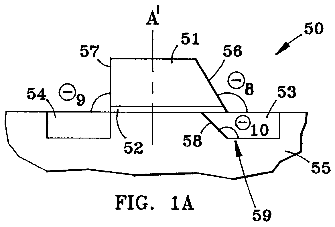
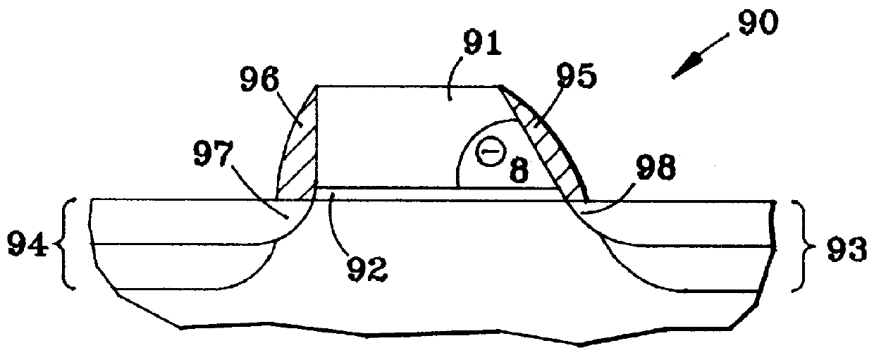
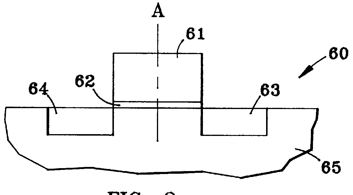
Polysilicon (also referred to as polycrystalline silicon) can be formed using chemical vapor deposition (CVD), or low pressure chemical vapor deposition (LPCVD), as well as other known processes. Polysilicon is a solid composed of a myriad of small single crystal regions. In FIG. 1A a cross section of an embodiment of the present invention is shown. The field effect transistor (FET) 50 is formed in a substrate 55 and comprises a gate electrode 51, a gate oxide 52, a source region 54 and a drain region 53. The substrate 55 may be a silicon substrate, for example. The source and drain regions 54, 53 can be defined by implantation of dopants. The doped regions may be implanted vertically or angled. Well suited for n-type do...


PUM


Abstract

Disclosed is an asymmetric field effect transistor which comprises a first region serving as source, a second region serving as drain, a thin gate oxide and a gate electrode. The gate electrode is asymmetric and one of its sidewalls is sloped. The second region extends underneath said sloped sidewall. The part of said second region which extends underneath said gate electrode is less doped than the remaining part of said second region. Furthermore, said second region has a sloped junction edge underneath said gate electrode.

Description

1. Cross-Reference to Related Patent ApplicationsThis patent application is related to U.S. patent application entitled "Asymmetrical Resist Sidewall", and U.S. patent application entitled "Selective Reduction of Sidewall Slope on Isolation Edge", both filed on the same day as the instant patent application and presently assigned to the assignee of the instant application and the disclosure of which is incorporated herein by reference.2. Field of the InventionThis invention relates to asymmetric field effect transistors (FETs) having a lightly doped drain.3. Description of Related ArtIn electronic component manufacture and in particular integrated circuit silicon wafer manufacturing, the key factor in delineating small patterns in the wafer is the shape of the resist pattern. The following description will be directed to integrated circuit silicon wafer manufacture and silicon devices but it will be appreciated by those skilled in the art that the invention may be applied to the man...

Claims


Application Information

Patent Timeline
IPC IPC(8): H01L21/266H01L29/40H01L21/336H01L29/423H01L21/02H01L29/78H01L21/3213H01L29/66H01L21/027H01L21/8234H01L27/088
CPCH01L21/266H01L21/32139H01L29/42376H01L29/66545H01L29/66598H01L29/66659H01L29/7835H01L21/0274
Inventor WHEELER, DONALD C.GAMBINO, JEFFREY P.HSU, LOUIS L.MANDELMAN, JACK A.MIH, REBECCA D.
Owner IBM CORP
Why Eureka
Try Eureka