Adaptable scan chains for debugging and manufacturing test purposes

a scan chain and manufacturing technology, applied in the direction of solid-state devices, semiconductor devices, instruments, etc., can solve the problems that multiple scan chains in the jtag environment do not provide much benefit, and achieve the effects of reducing scan time operation, preventing design errors in scan chain construction, and avoiding a change in the configuration of functional blocks

Inactive Publication Date: 2000-01-25
SAMSUNG ELECTRONICS CO LTD
View PDF28 Cites 63 Cited by
  • Summary
  • Abstract
  • Description
  • Claims
  • Application Information

AI Technical Summary

Benefits of technology

For chip debugging purposes during prototype development it is advantageous to have multiple scan chains instead of one single long chain for a chip. The scan chains not selected do not change their state with multiple scan chains. Having a selectable scan chain for one or more functional blocks provides a number of advantages. The advantages include: allowing for debugging to be focused on functional blocks; preventing design errors in scan chain construction from affecting scan chains in other functional blocks; reducing scan time operation by focusing on functional blocks; and avoiding a change in the configuration of the functional blocks which are not being scanned while allowing changes in the functional block to be scanned.

Problems solved by technology

However, multiple scan chains in the JTAG environment do not provide much benefit when manufacturing test time becomes important.

Method used


Image

  • Adaptable scan chains for debugging and manufacturing test purposes
  • Adaptable scan chains for debugging and manufacturing test purposes
  • Adaptable scan chains for debugging and manufacturing test purposes

Examples


Embodiment Construction

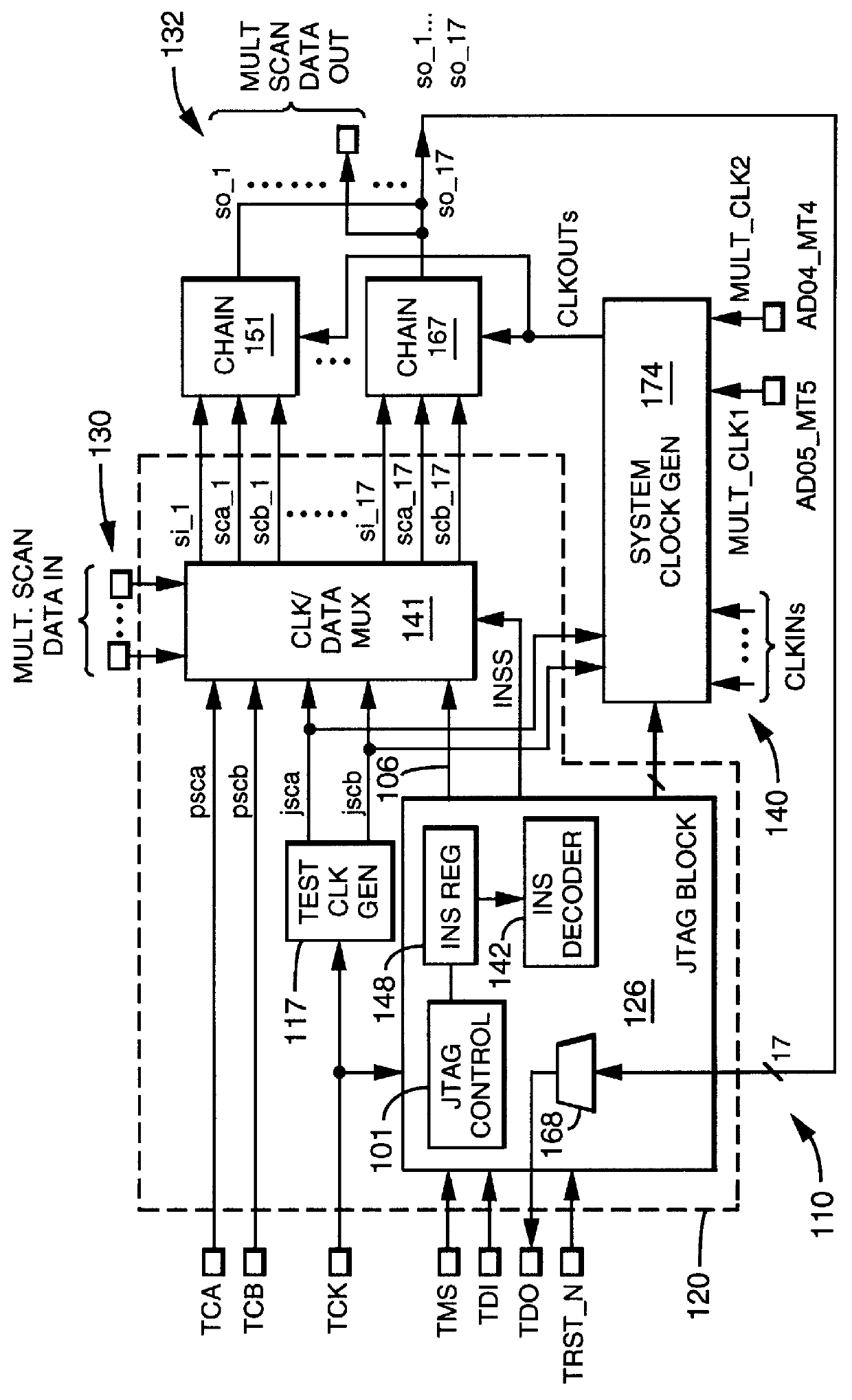
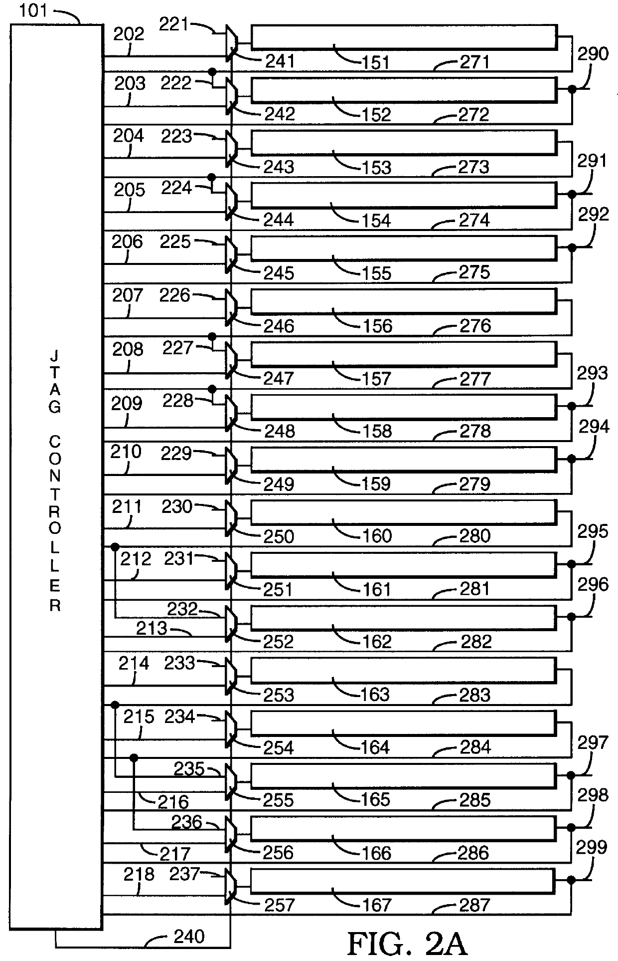
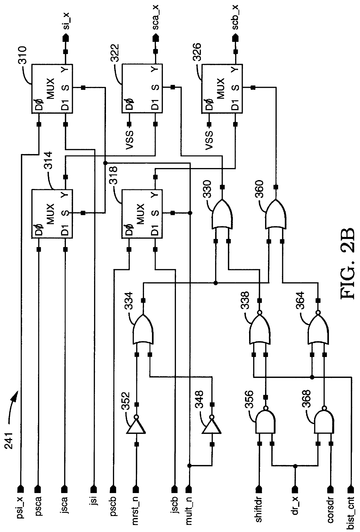
FIG. 1 is a block diagram of an integrated circuit (IC) 110. IC 110 includes testing circuitry to facilitate the integrated circuit testing. In some embodiments, the integrated circuit chip is a Multimedia Signal Processor (MSP.TM.) developed at Samsung Semiconductor, Inc. of San Jose Calif. That processor is described in U.S. patent application Ser. No. 08 / 699,303 filed Aug. 19, 1996 by C. Reader et al. and entitled "Methods and Apparatus for Processing Video Data". That patent application is incorporated herein by reference. The MSP testing circuitry is described in detail in Appendices A-B herein. In particular, Appendix B includes Verilog code for the testing circuitry.

The testing circuitry includes test control circuit 120 (FIG. 1). Circuit 120 can function as a control circuit for boundary scan testing in accordance with the JTAG standard.

In addition to boundary scan testing, test control circuit 120 is suitable for internal testing as defined below.

IC 110 includes 5 pins defi...


PUM


Abstract

Scan chains to support debugging and manufacturing test modes for integrated circuit chips are made adaptable. Scan chains may be configured either in a multiple scan chain JTAG mode or in a multiple independent and parallel scan chain mode. The configuration transition between the scan modes is made by private instructions implemented in a JTAG controller, which supports the IEEE 1149.1 standard.

Description

COPYRIGHT NOTICEA portion of the disclosure of this patent document contains material which is subject to copyright protection. The copyright owner has no objection to the facsimile reproduction by anyone of the patent document or the patent disclosure, as it appears in the Patent and Trademark Office patent file or records, but otherwise reserves all copyright rights whatsoever.A recent development in integrated circuit testing is the use of the JTAG (Joint Test Action Group) test port for in situ testing of integrated circuit chips mounted on a circuit board. The JTAG standard has been adopted by the Institute of Electrical and Electronics Engineers and is now defined as IEEE Standard 1149.1, IEEE Standard Test Access Port and Boundary-Scan Architecture, which is incorporated herein by reference. The IEEE Standard 1149.1 is explained in C. M. Maunder and R. E. Tulloss, "Test Access Port and Boundary-Scan Architecture" (IEEE Computer Society Press, 1990) which is also incorporated ...

Claims


Application Information

Patent Timeline
Patent Type & Authority Patents(United States)
IPC IPC(8): G01R31/3185G01R31/28G01R31/317G11C29/00H01L21/822H01L27/04
CPCG01R31/31705G01R31/318536G01R31/318563G11C29/00
Inventor BAEG, SANGHYEON
Owner SAMSUNG ELECTRONICS CO LTD
Why Eureka
Try Eureka