Process for defining a pattern using an anti-reflective coating and structure therefor

a technology of anti-reflective coating and pattern, applied in the field of microelectronic devices, can solve the problems of increased penetration, long exposure time, radiation leakage through the mask,

Inactive Publication Date: 2000-02-29
IBM CORP
View PDF4 Cites 113 Cited by
  • Summary
  • Abstract
  • Description
  • Claims
  • Application Information

AI Technical Summary

Problems solved by technology

Problems encountered in further device miniaturization include obtaining desired resolution in the radiation source and improved focusing resolution and depth of focus of the radiation on the photoresist.
Other problems encountered include radiation leakage through the mask.
Additionally, the problem of long exposure time exists to increase the penetration of the UV radiation through planarization layers.
Further problems include the ability of the patterns formed in the resist to withstand high power dry processes without the loss of the image integrity.
However, a common problem encountered as structure size has decreased is that thinner layers of photoresist must be used to ensure, among other things, that depth of focus requirements of the exposure tool are met.
The further photochemical reactions resulting from the UV radiation reflected off of the surface typically result in uneven exposure of the photoresist.
As a result, the structure which was intended to be created by the mask will not be created, as particularly evidenced by inconsistent feature dimensions.
This results in device error and possibly failure.
As the photoresist is exposed to UV radiation, when the anti-reflective coating or ARC is an inorganic material it bounces back any light at about a

Method used


Image

  • Process for defining a pattern using an anti-reflective coating and structure therefor
  • Process for defining a pattern using an anti-reflective coating and structure therefor
  • Process for defining a pattern using an anti-reflective coating and structure therefor

Examples


Embodiment Construction

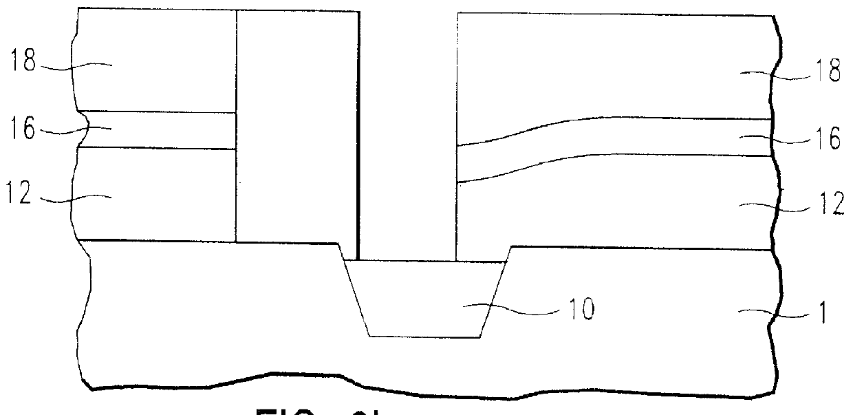
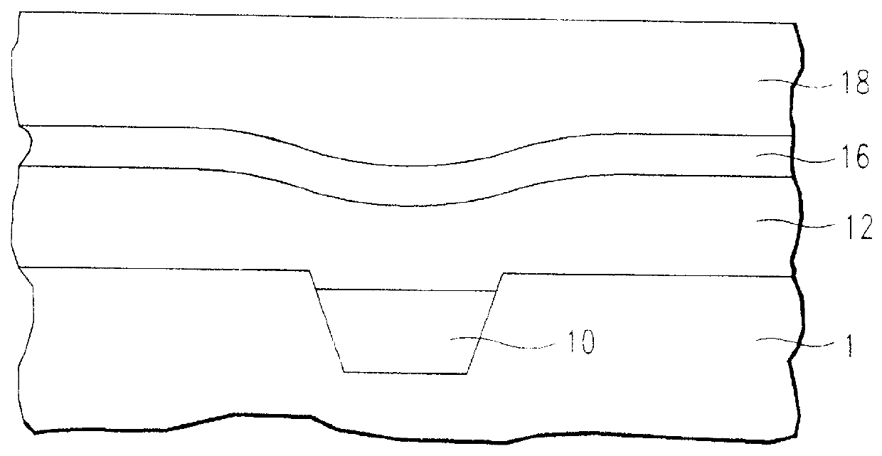
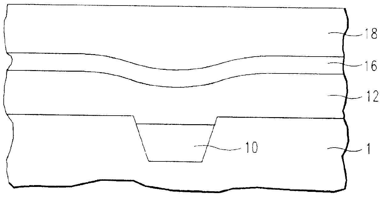
The present invention provides for defining a pattern in a surface. Although the present invention may be used to define a pattern in a variety of surfaces, the present invention is especially suitable for defining a pattern in a semiconductor substrate and especially a substrate having a non-planar topology. In order to facilitate an understanding of the present invention, reference will be made to the figures which illustrate a diagrammatic representation of the steps of carrying out the process of the present invention. According to the present invention, a layer 12 of a hard mask material is provided on a semiconductor substrate 1. The semiconductor substrate is typically silicon but can be any other semiconductor material such as group III-V semiconductor. The term "hard mask" material as known in the prior art refers to an inorganic masking material. The layer of hard mask material is preferably silicon dioxide obtained from tetraethyloxysilane (TEOS). The TEOS is deposited by...


PUM

PropertyMeasurementUnit
Thicknessaaaaaaaaaa
Semiconductor propertiesaaaaaaaaaa
Reflectionaaaaaaaaaa

Abstract

A pattern in a surface is defined by providing on the surface a hard mask material; depositing an anti-reflective coating on the hard mask material; applying a photoresist layer on the anti-reflective coating; patterning the photoresist layer, anti-reflective layer and hard mask material; and removing the remaining portions of the photoresist layer and anti-reflective layer; and then patterning the substrate using the hard mask as the mask. Also provided is a structure for defining a pattern in a surface which comprises a surface having a hard mask material thereon; an anti-reflective coating located on the hard mask material; and a photoresist located on the anti-reflective coating. Also provided is an etchant composition for removing the hard mask material which comprises an aqueous composition of HF and chlorine.

Description

The present invention is concerned with a process for defining a pattern in a surface and especially concerned with employing an anti-reflective coating. Furthermore, the present invention is concerned with a structure suitable for defining a pattern in a substrate wherein the structure includes an anti-reflective coating.BACKGROUND OF INVENTIONMicroelectronic devices used in fabricating integrated circuits are manufactured by employing photolithographic techniques. Fabricating various structures, particularly electronic device structures, typically involves depositing at least one layer of a photosensitive material, generally known as a photoresist material, on a substrate. The photoresist material may then be patterned by exposing it to radiation of a certain wavelength to alter characteristics of the photoresist material. In many instances, the radiation is from ultraviolet range of wavelengths causing desired photochemical reactions to occur within the photoresist. The photochem...

Claims


Application Information

Patent Timeline
IPC IPC(8): H01L21/027H01L21/28H01L21/02H01L21/3213
CPCH01L21/0276H01L21/28123H01L21/32139
Inventor ADKISSON, JAMES W.CATERER, MICHAELMARSH, JAMES T.NG, HUNGOBERSCHMIDT, JAMES M.RANKIN, JED H.
Owner IBM CORP
Why Eureka
Try Eureka