Embedded static random access memory for field programmable gate array

a random access memory and gate array technology, applied in the field of embedded static random access memory for field programmable gate array (fpga) architecture, can solve the problems of inconvenient use, low memory utilization rate, and inability to detect faulty hardware by configuration test,

Inactive Publication Date: 2000-04-11
MICROSEMI SOC
View PDF46 Cites 94 Cited by
  • Summary
  • Abstract
  • Description
  • Claims
  • Application Information

AI Technical Summary

Benefits of technology

It is a further object of the present invention to provide outputs from the an SRAM block that can set to a high impedance state so that the SRAM blocks may be connected into deeper and wider memories.
It is a further object of the present invention to provide an address collision detector to resolve the conflict between the timing signals when both the read port and the write port of an SRAM block are accessed close to simultaneously.
It is yet another object of the present invention to provide an SRAM block for an FPGA including a sense amplifier that provides for shifting the duration of the read access time between the set-up time and the clock-to-out time.
In a preferred embodiment, there eight fully independent blocks of 2K bit SRAM blocks, wherein each SRAM block is organized as 256 words of 8 bits, disposed between two upper multiple logic arrays and the two lower multiple logic arrays. The eight SRAM blocks are further divided into two groups such that the SRAM blocks in each of the groups are substantially contiguous to the extent that the address busses, data busses, and control signal lines of each of the user-configurable SRAM blocks in a group can be commonly connected by user-programmable elements at their edges to facilitate directly combining the user-configurable SRAM blocks in a group into wider and / or deeper user-assignable memory configurations.

Problems solved by technology

Both of these solutions are less than satisfactory.
Using external SRAMs with FPGA designs is undesirable for several reasons.
Separate memory chips are expensive, require additional printed circuit board space, and consume I / O pins on the FPGA itself.
Also, a separate memory chip is required to implement each memory function, thereby further increasing the cost.
This substantially degrades both the performance and flexibility of the FPGA by consuming a considerable amount of logic array resources, and imposes critical paths that are quite long for even a small memory block.
While this distributed SRAM approach is an improvement in density and is flexible for building larger memories, it is still slow and consumes logic array resources.
On its 4000 E Series parts, Xilinx also offers the ability to configure two configurable logic blocks to emulate a dual ported 16.times.1 SRAM block, however, this design still carries with it performance and flexibility degradation.
However, providing memory by having other than explicitly dedicated SRAM blocks included in the FPGA has not proved satisfactory.
However, the local interconnect structure disclosed in Wilton suffers performance problems due to excessive flexibility in the interconnect architecture.
This approach builds the flexibility of different widths and depths into the SRAM block, but at a significant performance cost since the access time of an embedded array block is very slow for a memory of the size and the technology in which it is built.
One of the significant issues in providing SRAM blocks in an FPGA architecture is the ability to connect these blocks to one another to form memories that either include more words (greater depth) than in a single block or have a longer word length (greater width) than in a single block.
Unfortunately, this approach required array routing resources to interconnect SRAM blocks into deeper and wider configurations.
Further, one of the problems associated with using a dual ported SRAM, is the behavior of the dual ported SRAM when both the read and write ports simultaneously access the same address.
Testing the fixed data stored in the SRAM is of critical concern, because in high reliability applications the undetected occurrence of a changed bit is not considered acceptable.

Method used


Image

  • Embedded static random access memory for field programmable gate array
  • Embedded static random access memory for field programmable gate array
  • Embedded static random access memory for field programmable gate array

Examples


Embodiment Construction

Those of ordinary skill in the art will realize that the following description of the present invention is illustrative only and not in any way limiting. Other embodiments of the invention will readily suggest themselves to such skilled persons.

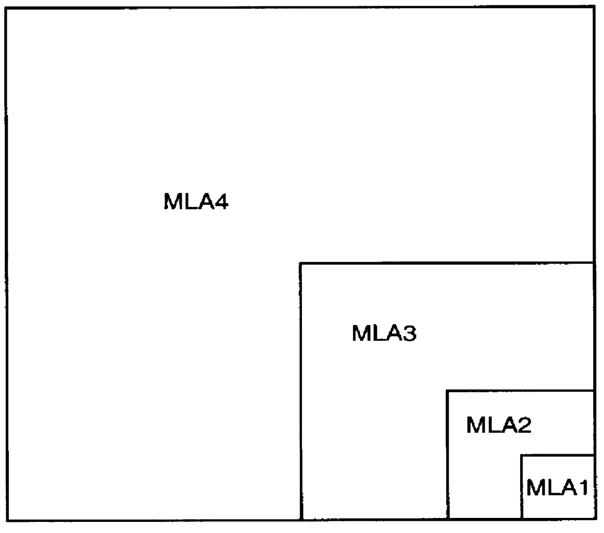
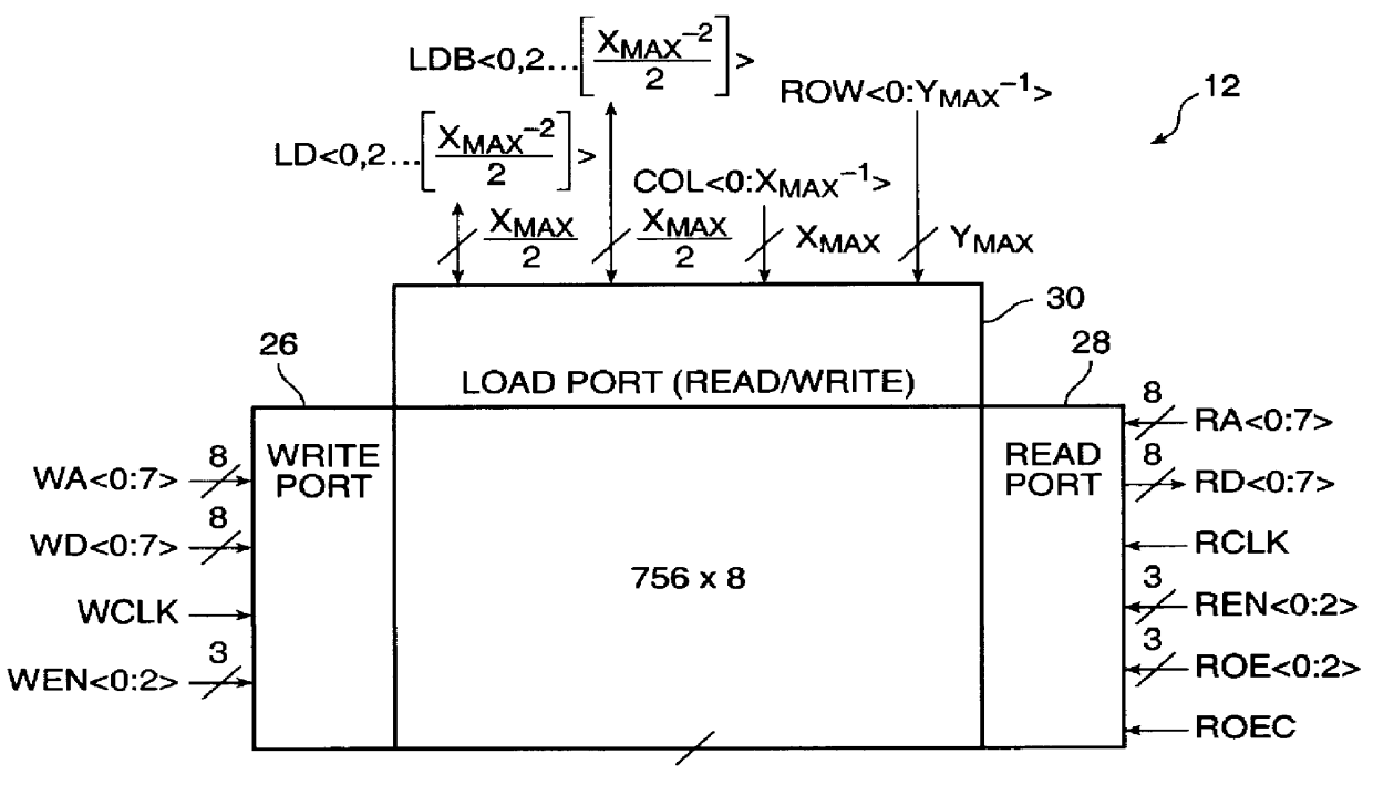
According to the present invention, in FIG. 1 a block diagram of the FPGA core 10 in a flexible, high-performance SRAM based FPGA architecture having user-assignable SRAM blocks 12 according to the present invention is illustrated. The FPGA core 10 includes a plurality of logic function modules disposed within a multi-level architecture (MLA) of routing resources. The blocks 14-1 through 14-4 in FPGA core 10 illustrate a grouping of logic modules in the MLA termed MLA4. In the preferred embodiment, there are approximately 50K gates combined in blocks 14-1 through 14-4. The SRAM blocks 12 comprise 16K bits of user-assignable SRAM divided into eight dedicated blocks of 2K bits. The user-assignable SRAM blocks 12 will be more fully described bel...


PUM


Abstract

A dual ported (simultaneous read / write) SRAM block with an additional load port that interacts with the circuitry employed in the loading and testing of the configuration data of the FPGA core is disclosed. Each SRAM block contains circuits in both the read port and the write port that permit the SRAM blocks to be connected into deeper and wider configurations by without any additional logic as required by the prior art. An address collision detector is provided such that when both read and write ports in the SRAM block access the same address simultaneously a choice between the data being read can be made between the data presently in the SRAM block or the new data being written to the SRAM block.

Description

1. Field of the InventionThe present invention is related to a field programmable gate array (FPGA) architecture. More particularly, the present invention is related to an FPGA having embedded static random access memory (SRAM).2. The Prior ArtAs integrated circuit technology advances, geometries shrink, performance improves, and densities increase. This trend makes feasible the design of systems of ever increasing complexity at ever decreasing cost. This is especially true in logic products such as Application Specific Integrated Circuits (ASICs), Complex Programmable Logic Devices (CPLDs), and Field Programmable Gate Arrays (FPGAs).The need for integrating fast, flexible, inexpensive memory into these logic products to provide memory for a variety of purposes such as register files, FIFOs, scratch pads, look-up tables, etc. has become more apparent, because there are significant cost and performance savings to be obtained by integrating this functionality directly into for example...

Claims


Application Information

Patent Timeline
Patent Type & Authority Patents(United States)
IPC IPC(8): G11C8/16G11C8/00G11C11/00G06F11/22
CPCG11C11/005G11C8/16G06F11/2289
Inventor PLANTS, WILLIAM C.JOSEPH, JAMES DEANBELL, ANTONY G.
Owner MICROSEMI SOC
Why Eureka
Try Eureka