Thin film dielectric device

a thin film dielectric and dielectric technology, applied in solid-state devices, transistors, capacitors, etc., can solve the problems of large interface level, difficult epitaxial growth of the lower electrode, and inability to highly match the electrode and the dielectric thin film at the interfa

Inactive Publication Date: 2000-05-09
KK TOSHIBA
View PDF4 Cites 58 Cited by
  • Summary
  • Abstract
  • Description
  • Claims
  • Application Information

AI Technical Summary

Problems solved by technology

However, in a thin film dielectric device of which Ru or an oxide thereof is used for a lower electrode, a large amount of interface levels will take place due to ion defeats resulting from the mismatching of the interface an electrode and a dielectric thin film.
It is very difficult to epitaxially grow the lower electrode composed of a conductive perovskite oxide on a plug composed of poly-silicon in a good condition.
Thus, the electrode and the dielectric thin film cannot be highly matched at the interface thereof.
However, in such a structure, the morphology degrades at the interface of the lower electrode and the

Method used


Image

  • Thin film dielectric device
  • Thin film dielectric device
  • Thin film dielectric device

Examples


third embodiment

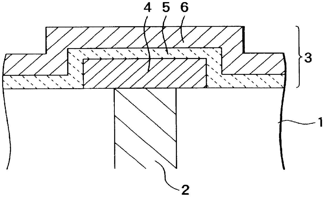
As shown in FIG. 3, a SiO.sub.2 insulation film 7 was formed for 300 nm on an Si substrate 1 having a plug 2 (formed by the selective growing method) by plasma TEOS method. A capacitor trench 8 was formed on the SiO.sub.2 insulation layer 7 by lithograph process.

Next, a SrRuO.sub.3 film for 30 nm as a lower electrode 4 was deposited on the SiO.sub.2 insulation layer 7 including the capacitor trench 8 (temperature of substrate=873 K). Thereafter, the surface was flatted by CMP and cells were separated. Before the SrRuO.sub.3 film was formed, the cleaning process as with the first embodiment was performed.

Thereafter, a Ba.sub.0.5 Sr.sub.0.5 TiO.sub.3 film for 20 nm as a dielectric thin film 5 was formed on the lower electrode 4 by RF magnetron spatter method. A SrRuO.sub.3 film for 30 nm as an upper electrode 6 was deposited on the dielectric thin film 5. Thus, a thin film capacitor for a DRAM was fabricated.

The section of the resultant thin film capacitor was observed by the electron...

fourth embodiment

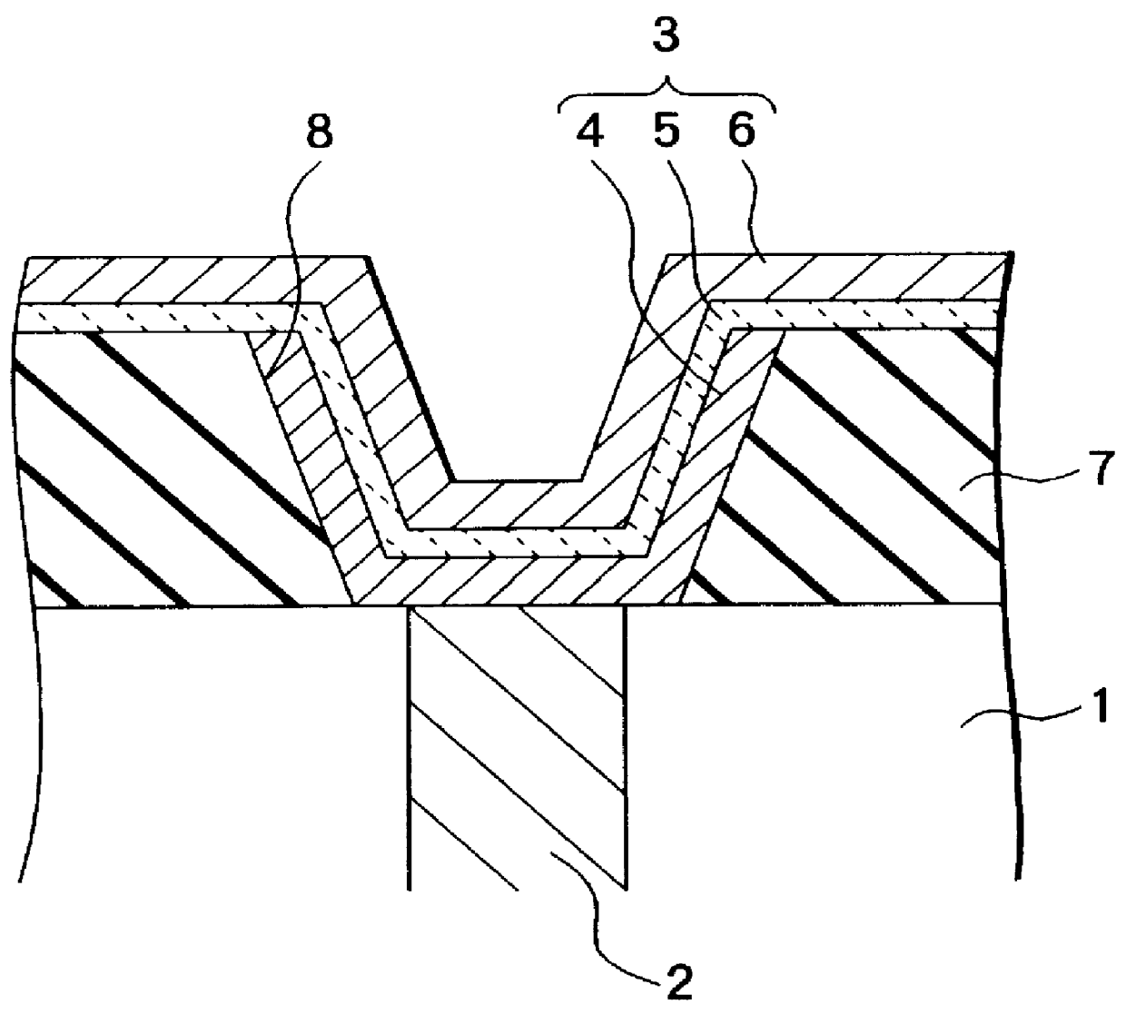
As with the third embodiment, a SiO.sub.2 insulation film 7 was formed for 300 nm on an Si substrate 1 having a plug 2 by plasma TEOS method. A capacitor trench 8 was formed on the SiO.sub.2 insulation layer 7 by lithograph process.

Next, a La.sub.0.5 Sr.sub.0.5 CoO.sub.3 film for 30 nm as a lower electrode 4 was deposited on the SiO.sub.2 insulation layer 7 including the capacitor trench 8 (temperature of substrate=873 K). Thereafter, the surface was flatted by CMP and cells were separated. Before the La.sub.0.5 Sr.sub.0.5 CoO.sub.3 film was formed, the cleaning process as with the first embodiment was performed.

Thereafter, a Ba.sub.0.5 Sr.sub.0.5 TiO.sub.3 film for 20 nm as a dielectric thin film 5 was formed on the lower electrode 4 by RF magnetron spatter method. A La.sub.0.5 Sr.sub.0.5 CoO.sub.3 film for 30 nm as an upper electrode 6 was deposited on the dielectric thin film 5. Thus, a thin film capacitor for a DRAM was fabricated.

The section of the resultant thin film capacitor...

fifth embodiment

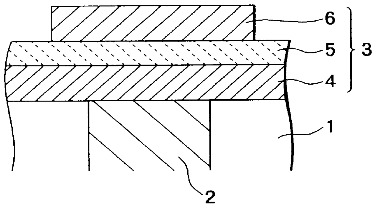
A Ba.sub.0.12 Sr.sub.0.88 TiO.sub.3 film for 20 nm as a dielectric thin film was formed on a SrRuO.sub.3 film (lower electrode) formed in the same manner as the first embodiment. A SrRuO.sub.3 film for 30 nm as an upper electrode was deposited on the dielectric thin film. Thus, a thin film capacitor for a DRAM was fabricated.

The section of the resultant thin film capacitor was observed by the electron microscope (TEM). As a result, the laminate film of the lower electrode, the dielectric thin film, and the upper electrode was having columnar grains of which the size of each layer in the direction of the surface of the substrate was the same and the crystal orientation of each layer was the same. When the X ray diffraction of the thin film capacitor was measured, the peaks of the SrRuO.sub.3 film and the Ba.sub.0.12 Sr.sub.0.88 TiO.sub.3 film overlapped. The estimated lattice constant was 0.398 nm.

The electric characteristics of the thin film capacitor according to the fifth embodime...


PUM


Abstract

A thin film dielectric device is disclosed, that comprises a substrate, a lower electrode formed on the substrate and composed of a laminate film having columnar grains that have grown in a vertical to a surface of the substrate, a dielectric thin film formed on the lower electrode and composed of a perovskite oxide, the dielectric thin film being a polycrystalline film having columnar grains that have successively grown from the columnar grains of the lower electrode and that takes over a crystal orientation of the lower electrode, the lattice constant of the lower electrode being matched with the lattice constant of the dielectric thin film at the interface therebetween with the columnar grains, and an upper electrode formed on the dielectric thin film. The lattice matching of the columnar grains solves problems of the increase of the leak current of the thin film dielectric device and the degradation of the dielectric breakdown resistance. In addition, the polycrystalline film having the columnar grains that succeed at the interface of the electrode/dielectric thin film can be properly formed on the semiconductor substrate such as Si substrate. Thus, the thin film dielectric device according to the present invention can be applied to a real LSI circuit and so forth.

Description

1. Field of the InventionThe present invention relates to a thin film dielectric device having a dielectric thin film composed of a perovskite oxide.2. Description of the Related ArtIn recent years, materials with high permittivity and ferroelectricity of thin film dielectric devices (thin film capacitors) that are disposed on large storage DRAMs and non-volatile ferroelectricity memories (FRAMs) and device structures thereof have been intensively studied. For example, the dielectric constants of perovskite oxides such as SrTiO.sub.3 (hereinafter referred to as STO) and Ba.sub.1-x Sr.sub.x TiO.sub.3 (hereinafter referred to as BSTO) are much larger than the dielectric constants of conventional materials such as SiO.sub.2, Si.sub.3 N.sub.4, and Ta.sub.2 O.sub.5. Thus, even if memory cells are finely structured, a sufficient storage capacity of electric charges can be obtained. In addition, a desired storage capacitance can be accomplished without need to use a complicated capacitor s...

Claims


Application Information

Patent Timeline
IPC IPC(8): H01L21/02
CPCH01L28/75H01L28/55H01L28/60
Inventor IZUHA, MITSUAKIFUKUSHIMA, NOBURUABE, KAZUHIDE
Owner KK TOSHIBA
Why Eureka
Try Eureka