Peripheral buses for integrated circuit

a technology of integrated circuits and peripheral buses, applied in the field of integrated circuits, can solve the problems of capacitive load, power consumption is very important, and adversely affect the operation of system buses

Inactive Publication Date: 2000-05-16
ARM LTD
View PDF1 Cites 159 Cited by
  • Summary
  • Abstract
  • Description
  • Claims
  • Application Information

AI Technical Summary

Benefits of technology

Since the integrated circuit in accordance with the present invention has two peripheral buses, with the first peripheral bus operating at a higher clock speed than the second peripheral bus, there is now a choice as to which peripheral bus any particular peripheral unit is connected to. The power consumption of each peripheral bus is proportional to the clock frequency and capacitance, and hence, for any particular loading, the peripheral bus operating at a higher clock speed will tend to consume more power than the peripheral bus operating at a lower clock speed. Accordingly, the integrated circuit in accordance with the present invention, through the provision of first and second peripheral buses operating at different clock speeds, provides a great deal of flexibility for reducing the power consumption of the integrated circuit as compared with a similar integrated circuit having only one peripheral bus. To optimise the power consumption savings, each peripheral unit is connected to the slowest peripheral bus appropriate for that peripheral unit. The capacitive load on the first, higher speed, peripheral bus is kept to a minimum by connecting as few peripheral units to that higher speed bus as possible. Although this may mean that a relatively large number of peripheral units are connected to the second, slower, peripheral bus, and hence the capacitive load of the second peripheral bus is high, since the clock speed is slower than that of the first peripheral bus, the power consumption is still acceptable.
In preferred embodiments, a number of said peripheral units require a common clock speed and are connected to said second peripheral bus, said second peripheral bus being arranged to operate at said common clock speed, thereby avoiding the requirement for separate clock resynchronisation logic to be provided at each of said number of peripheral units. This approach saves on logic and also saves power, since the need for multiple synchronisers associated with each peripheral unit is avoided, and instead the resynchronisation is achieved centrally by clock resynchronisation logic provided within the bridge logic.
In preferred embodiments of the present invention, two peripheral buses are provided within the integrated circuit. However, in alternative embodiments, the integrated circuit further comprises one or more additional peripheral buses arranged to operate at clock speeds different to the clock speeds of said first and said second peripheral buses. It will be appreciated that this provides further flexibility in the location of each peripheral unit. Hence, if there are a number of different groups of peripheral units, with each group containing peripheral units arranged to operate at a particular clock speed, then a separate peripheral bus can be provided for each group, and can be arranged to operate at the appropriate clock speed, thereby avoiding the need for any clock resynchronisation to be performed at a particular peripheral unit. As mentioned earlier, this yields savings in both logic and power consumption.

Problems solved by technology

It enables multiple peripheral units to be connected without loading the main system bus, which would adversely affect the operation of the system bus.
When developing integrated circuits, the issue of power consumption is very important.
The power consumption of each peripheral bus is proportional to the clock frequency and capacitance, and hence, for any particular loading, the peripheral bus operating at a higher clock speed will tend to consume more power than the peripheral bus operating at a lower clock speed.
Although this may mean that a relatively large number of peripheral units are connected to the second, slower, peripheral bus, and hence the capacitive load of the second peripheral bus is high, since the clock speed is slower than that of the first peripheral bus, the power consumption is still acceptable.

Method used


Image

  • Peripheral buses for integrated circuit
  • Peripheral buses for integrated circuit
  • Peripheral buses for integrated circuit

Examples


Embodiment Construction

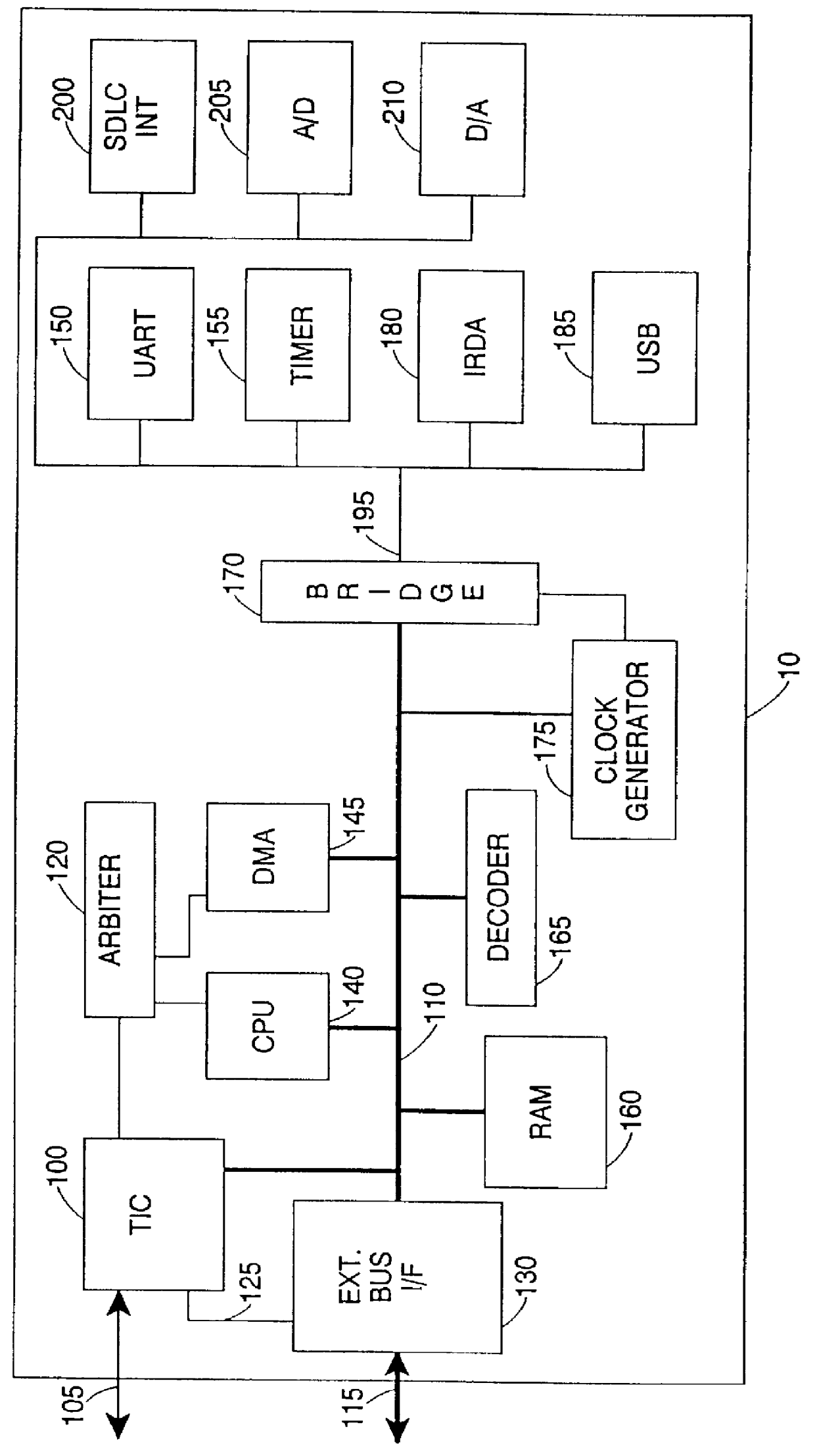
FIG. 1 illustrates a typical prior art integrated circuit, taking the form of a microcontroller chip 10. The chip 10 has a system bus 110 and a peripheral bus 195 connected via a bridge circuit 170. For the sake of illustration, these buses will be considered to operate in accordance with the "Advanced Microcontroller Bus Architecture" (AMBA) specification developed by ARM Limited. The AMBA specification defines an on-chip communication standard for designing high performance 32-bit and 16-bit embedded microcontrollers, with the system bus 110 being used for high performance system modules, whilst the peripheral bus is used for low power peripheral devices. The high performance system bus 110 is able to sustain the external memory bandwidth, with the CPU and other Direct Memory Access devices residing on the system bus, whilst a bridge circuit 170 connects the system bus to a narrower peripheral bus 195 on which the low bandwidth peripheral devices are located. The bridge circuit 17...


PUM


Abstract

The present invention provides an integrated circuit comprising a system bus to which a processor is connectable, and first and second peripheral buses to which peripheral units used by said processor are connected, the first peripheral bus operating at a higher clock speed than the second peripheral bus. Further, the integrated circuit comprises bridge logic for providing an interface between the system bus and the peripheral buses to enable signals to be passed between the system bus and the peripheral buses, the bridge logic comprising clock resynchronisation logic for synchronising the system bus and the peripheral buses. Through the provision of first and second peripheral buses operating at different clock speeds, the integrated circuit of the present invention provides a great deal of flexibility for reducing the power consumption of the integrated circuit as compared with a similar integrated circuit having only one peripheral bus. Since the power consumption of each peripheral bus is proportional to the clock frequency and capacitance, significant power consumption savings can be realised by ensuring that each peripheral unit is connected to the slowest peripheral bus appropriate for that peripheral unit.

Description

1. Field of the InventionThe present invention relates to integrated circuits of the type having a system bus to which a processor is connectable and a peripheral bus to which one or more peripheral units are connected.2. Description of the Prior ArtIt is known to provide an integrated circuit with a system bus to be used for high performance system modules, and a peripheral bus to be used for low power peripheral devices. The system modules, such as a processor, a Direct Memory Access (DMA) controller, etc may typically be provided as part of the integrated circuit, but alternatively one or more of such system modules may be provided off-chip. Similarly, the peripheral devices that connect to the peripheral bus may be provided within the integrated circuit, or alternatively may be provided off-chip. However, for the peripheral devices that are provided off-chip, there will typically be provided some corresponding on-chip logic that is connected to the peripheral bus, and is used to...

Claims


Application Information

Patent Timeline
Patent Type & Authority Patents(United States)
IPC IPC(8): G06F13/40
CPCG06F13/405Y02B60/1235Y02B60/1228Y02D10/00
Inventor STEVENS, ASHLEY MILES
Owner ARM LTD
Why Eureka
Try Eureka