Intra-pixel frame storage element, array, and electronic shutter method including speed switch suitable for electronic still camera applications

Inactive Publication Date: 2000-05-30
FOVEON
View PDF35 Cites 61 Cited by
  • Summary
  • Abstract
  • Description
  • Claims
  • Application Information

AI Technical Summary

Benefits of technology

According to a second aspect of the present invention, a method for implementing an electronic shutter having a greatly reduced ADC sample rate requirem

Problems solved by technology

In the CCD art, techniques have been developed for preventing leakage and contamination due to minority carrier diffusion and leakage, but these techniques are not applicable to the CMOS sensor array because the silicon fabrication processes are different.
In still-camera applications with randomly-addressable CMOS active-pixel sensors, the problem of how to implement a short-exposure interval with a long readout interval exists.
There are two problems with this type of electronic shutter.
First, since each row scans a different time interval, there will be motion artifacts (the shape of moving objects will be d

Method used


Image

  • Intra-pixel frame storage element, array, and electronic shutter method including speed switch suitable for electronic still camera applications
  • Intra-pixel frame storage element, array, and electronic shutter method including speed switch suitable for electronic still camera applications
  • Intra-pixel frame storage element, array, and electronic shutter method including speed switch suitable for electronic still camera applications

Examples


Embodiment Construction

Those of ordinary skill in the art will realize that the following description of the present invention is illustrative only and not in any way limiting. Other embodiments of the invention will readily suggest themselves to such skilled persons.

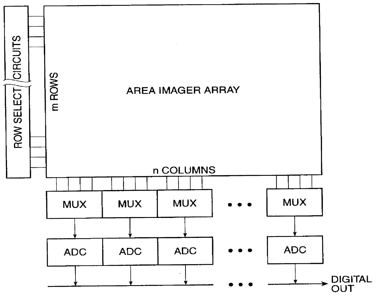
To facilitate an understanding of the present invention, an understanding of the operation of prior-art active-pixel area-array image sensors is helpful. Referring first to FIG. 1, a block diagram of a typical prior-art active-pixel area-array image sensor is presented. A pixel array comprises m rows each having n columns of pixel elements.

A row-select circuit (shown at the left side of the array) is provided to scroll through the rows so that the integration duration for each row is the same. For each row, the analog value out of each pixel is multiplexed to ADC circuits to digitize the output values and provide a stream of digital data representing the outputs of the pixels in that row.

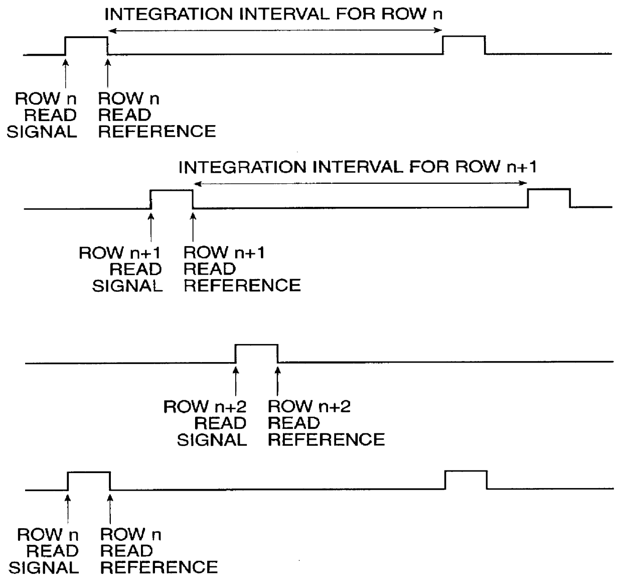
Referring now to FIG. 2, a timing diagram shows the com...


PUM


Abstract

A storage pixel sensor disposed on a semiconductor substrate comprises a MOS capacitor storage element having a diffusion terminal and a gate terminal. A speed node is connected to the diffusion terminal and biased at either a first control potential or a second control potential, the first potential selected to keep the MOS capacitor in a state of inversion, the second potential selected to keep the MOS capacitor in a state of depletion. A photodiode has an anode connected to a reference potential and a cathode. A semiconductor reset switch has a first terminal connected to the cathode and a second terminal connected to a reset reference potential. A semiconductor transfer switch has a first terminal connected to the cathode and a second terminal connected to the gate terminal of the capacitive storage element. A semiconductor amplifier has an input connected to the gate terminal of the capacitive storage element and an output. The semiconductor reset switch and the semiconductor transfer switch each have a control element connected to a control circuit for selectively activating the semiconductor reset switch and the semiconductor transfer switch. A light shield is disposed over a portion of the semiconductor substrate including the second terminal of the semiconductor transfer switch to prevent substantially all photons from entering the portion of the semiconductor substrate. Structures are present for preventing substantially all minority carriers generated in the semiconductor substrate from entering the portion of the semiconductor substrate. A plurality of storage pixel sensors are disposed in an array.

Description

1. Field of the InventionThe present invention relates to image sensor arrays. More particularly, the present invention relates to CMOS image sensor arrays for still camera applications and to methods for operating those arrays.2. The Prior ArtIntegrated image sensors are known in the art. Such sensors have been fabricated from charge-coupled devices (CCDs) and as bipolar and MOS image sensors.In the CCD imager art, on-chip frame storage capability has been employed previously. It has been motivated by the need to shift sensed charges out during a video frame time without letting them be contaminated by further exposure as the charges travel across the CCD array. Two storage techniques are commonly employed in the CCD imager art. According to the first technique, a second separate on-chip CCD array is provided under a light shield, and the entire image is quickly shifted along one dimension into the storage array, since shifting in one dimension is fast enough to avoid significant c...

Claims


Application Information

Patent Timeline
IPC IPC(8): H01L27/146H04N3/15H04N5/353H04N5/374H04N5/3745
CPCH01L27/14609H01L27/14623H04N5/37452H04N5/353H04N5/374H04N25/53H04N25/771H04N25/76
Inventor MERRILL, RICHARD B.
Owner FOVEON
Why Eureka
Try Eureka