Method for growing a silicon single crystal

a single crystal and silicon technology, applied in the direction of crystal growth process polycrystalline material growth, etc., can solve the problems of reducing yield, affecting the growth affecting the yield rate of silicon single crystals, so as to reduce the amount and reduce the effect of silica being melted ou

Inactive Publication Date: 2000-07-11
SUMITOMO MITSUBISHI SILICON CORP
View PDF9 Cites 32 Cited by
  • Summary
  • Abstract
  • Description
  • Claims
  • Application Information

AI Technical Summary

Benefits of technology

Where no magnetic field is applied to a melt as shown in FIG. 9, silica melts out from side-wall and bottom portions due to the flows occurring in the vicinity of the side-wall and bottom portions of the crucible. In this connection, however, when a horizontal magnetic field is applied to as shown in FIG. 10, the flows along the side-wall portions are suppressed, so that the oxygen concentration at the interface with the side-wall portions increases, resulting in the reduction in amount of silica being melted out. Moreover, when a vertical magnetic field is applied to the melting as shown in FIG. 11, the flows along the bottom are suppressed, with the result that the oxygen concentration at

Problems solved by technology

However, in actual operations, dislocation defects are produced during the pulling of a singe crystal, forcing the interruption of the pulling and the lowering of yield.
We made studies on the reduction in amount of foreign matters melted out from a quartz crucible and

Method used


Image

  • Method for growing a silicon single crystal
  • Method for growing a silicon single crystal
  • Method for growing a silicon single crystal

Examples


example 1

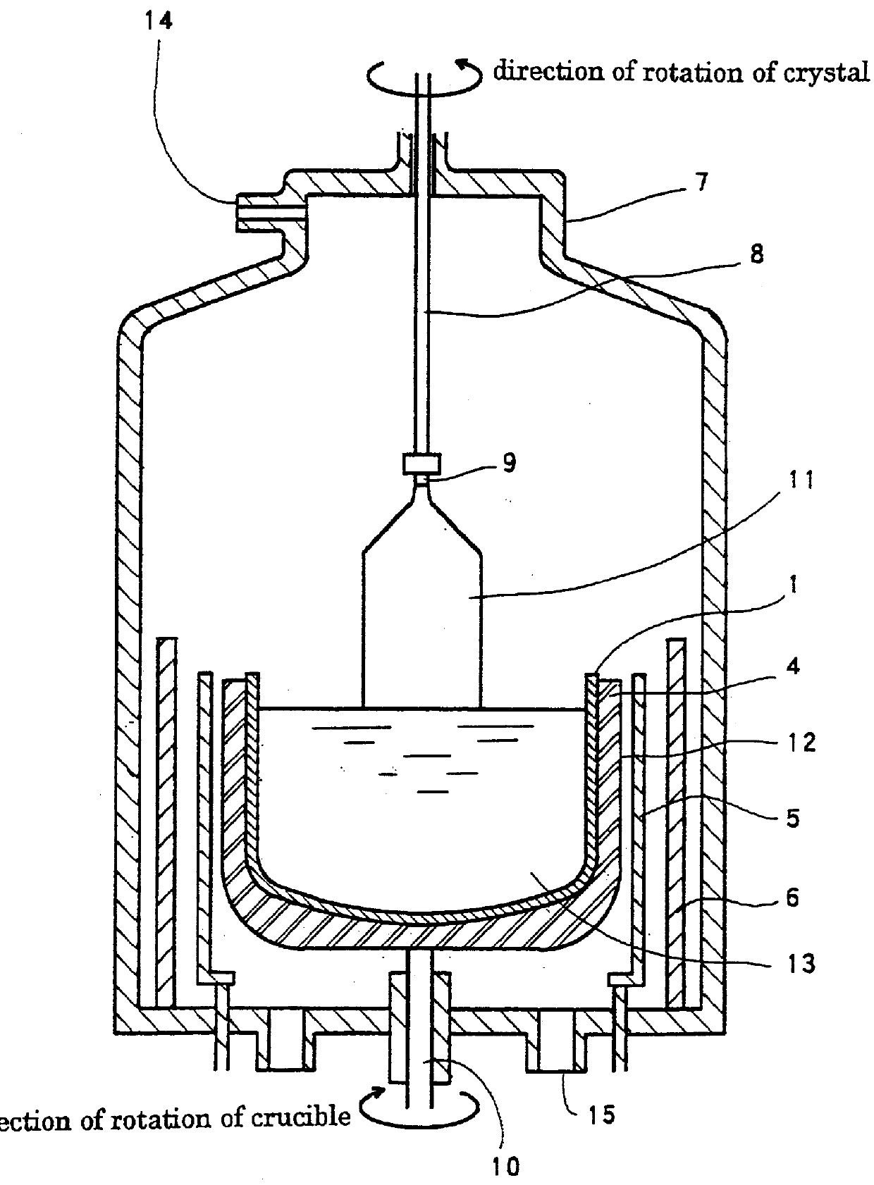
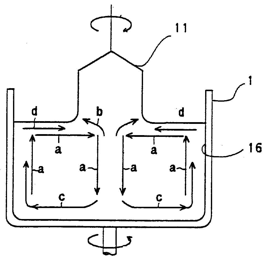
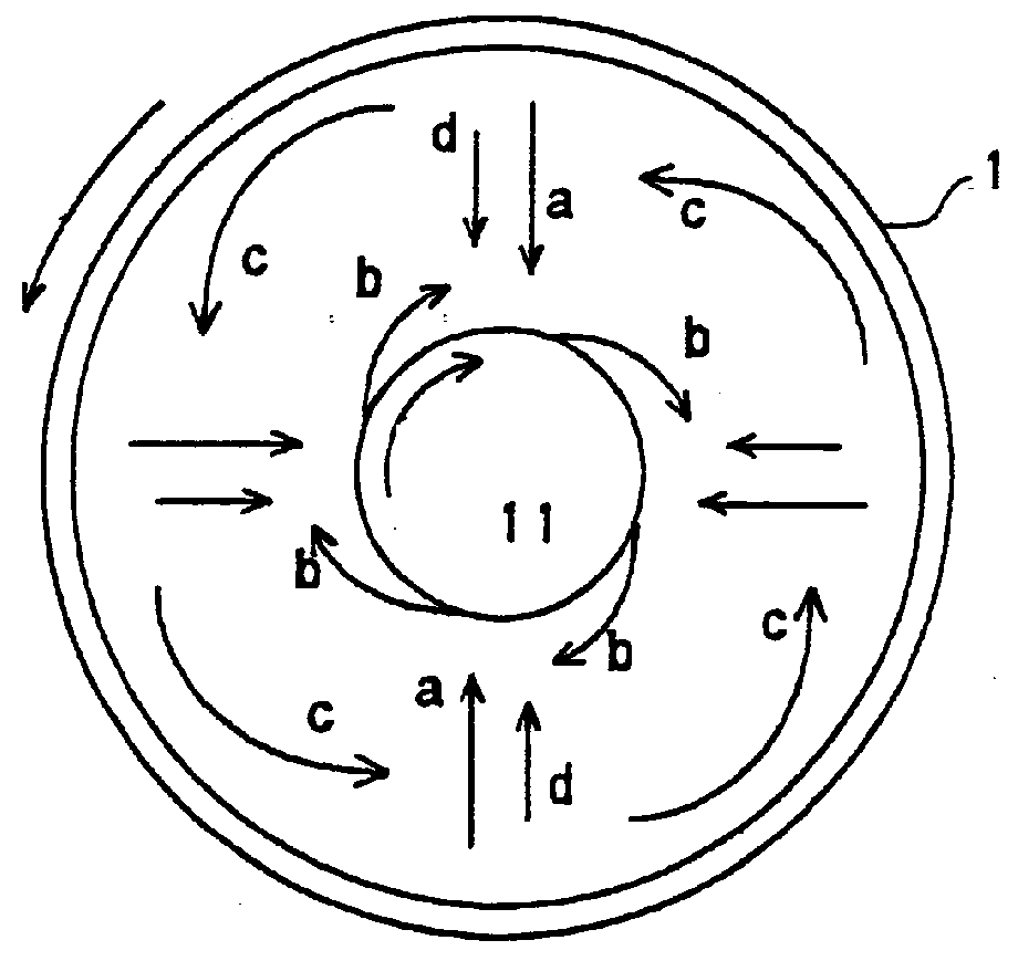
A single crystal pulling test was conducted using an apparatus of growing a silicon single crystal as shown in FIG. 8, wherein 100 kg of polysilicon was melted, while applying thereto the Cusp magnetic field in a manner as shown in FIG. 12.

The test conditions are as shown below.

Intended resistivity of single crystal: 10 .OMEGA.cm

Quartz crucible: an inner diameter of 22 inches (560 mm) and a height of 350 mm

Rotation speed of the crucible: 2 r.p.m. during melting, and 8 r.p.m. during growth

Power for heater: 100 kW during melting and 80 kW during growth

Intensity of an applied magnetic field: 400 gausses provided that no magnetic field was applied to during growth

Pulling diameter of single crystal: 6 inches

Pulling length of single crystal: 1300 mm and 1700 mm

Pulling speed of single crystal: 0.6 mm / minute

Rotation speed of single crystal: 15 r.p.m.

Pulling number of single crystals: 10

For comparison, the procedure of melting without application of any magnetic field in a manner as shown in...

example 2

A test was conducted under the same conditions as in Example 1, except that at the time of melting a silicon starting material, the intensity of an applied magnetic field was set at 400 gausses upon commencement of the melting and was changed to 500 gausses 7 hours after the commencement. At the pulling lengths of 1300 mm and 1700 mm, single crystals having dislocation defects were found to be zero in number. Thus, the case where the magnetic field was changed in its intensity in relation to time and the intensity of the magnetic field was changed at long time intervals without adversely influencing the suppression of flows of the melt is within the scope of the invention with respect to the use of static magnetic field.

As described hereinabove, when a silicon starting material is melted while applying thereto a static magnetic field according to the method of the invention, an amount of silica being melted out from a crucible into a melt can be educed, thereby preventing the occurr...


PUM


Abstract

A method for melting a silicon starting material can suppress silica (SiO2) from melting out from a quartz crucible wherein the silicon starting material is melted and can provide a high-quality silicon single crystal in a high yield. The growth method comprises melting the silicon starting material charged in the crucible while applying thereto a static magnetic field, contacting a seed crystal to a surface of the silicon melt, and pulling the seed crystal upwardly to solidify the contacted melt. The silicon starting material charged in the crucible, which is under melting, is applied with a static magnetic field such as a Cusp magnetic field, a horizontal magnetic field and/or a vertical magnetic field. The application can control heat convection occurring in the crucible during the course of the melting of the starting material, thereby obtaining a silicon single crystal having a reduced number of dislocation defects.

Description

This invention relates to a method for pulling and growing a highquality silicon single crystal, and more particularly, to a method for melting a silicon starting material which can well suppress silica (SiO.sub.2) from melting out from a quartz crucible in which the silicon starting material is melted.DESCRIPTION OF THE PRIOR ARTFor the manufacture of a silicon single crystal, there has been widely used a so-called Czochralski method wherein a highly pure silicon material is melted in an atmosphere of argon under reduced pressure, and a seed crystal is brought into contact with the melt surface and solidified while pulling upwardly.FIG. 1 is a longitudinal sectional view showing an apparatus of growing a silicon single crystal, which is solidified while pulling up according to the Czochralski method. In FIG. 1, a chamber 7 is under reduced pressure and in an atmosphere of pulling silicon single crystal 11. At the center of the chamber, a melting crucible 12 is placed, and a heater ...

Claims


Application Information

Patent Timeline
IPC IPC(8): C30B15/30C30B15/00C30B29/06C30B30/04H01L21/208
CPCC30B15/305Y10T117/1068Y10S117/917
Inventor KAWANISHI, SOUROKUYAMAMOTO, YOUICHI
Owner SUMITOMO MITSUBISHI SILICON CORP
Why Eureka
Try Eureka