Composite unit of optical semiconductor device and supporting substrate and method for mounting optical semiconductor device on supporting substrate

Inactive Publication Date: 2000-07-11
NEOPHOTONICS SEMICON GK
View PDF18 Cites 23 Cited by
  • Summary
  • Abstract
  • Description
  • Claims
  • Application Information

AI Technical Summary

Benefits of technology

Accordingly, an object of this invention is to provide a variety of composite units of an optical semiconductor device and a supporting substrate, which can readily be assembled with a satisfactory grade of accuracy in all the directions without requiring any particular skill and a significant amount of time and labor.

Problems solved by technology

1. The process for mounting an optical semiconductor device on a supporting substrate is complicated and requires a sizable amount of time and labor.
Particularly, the process for adjusting two marks is troublesome.
2. The accuracy in adjustment of the two pairs of the positioning marks is unsatisfactory, due to irregular reflection of infrared rays caused by roughness of the surfaces of the optical semiconductor device (2) and of the supporting substrate (1).
3. The accuracy in adjustment of the height of the active layer or the optical axis of an optical semiconductor device and the height of the center of the core of an optical fiber is unsatisfactory, because the height of the active layer or the optical axis of an optical semiconductor device inevitably varies depending on the thickness of a layer of solder which fixes the optical semiconductor device and the supporting substrate.

Method used


Image

  • Composite unit of optical semiconductor device and supporting substrate and method for mounting optical semiconductor device on supporting substrate
  • Composite unit of optical semiconductor device and supporting substrate and method for mounting optical semiconductor device on supporting substrate
  • Composite unit of optical semiconductor device and supporting substrate and method for mounting optical semiconductor device on supporting substrate

Examples


first embodiment

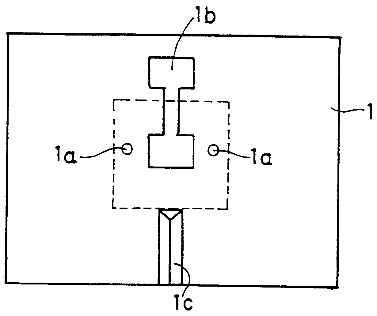
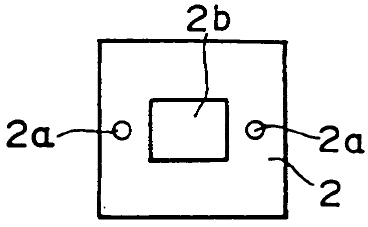
A composite unit of an optical semiconductor device and supporting substrate, wherein the supporting substrate has at least two recesses produced on the top surface thereof and lined by an electrode pattern made of an Au--Sn alloy layer or a piled layer of Cr / Ni / Au or of Ti / Pt / Au, and the optical semiconductor device has bumps made of an Au--Sn solder having a melting temperature less than the material of the electrode pattern and which bumps are produced at locations corresponding to the foregoing recesses, whereby the optical semiconductor device and the supporting substrate are fixed to each other with a good grade of accuracy by "the self alignment results" in the horizontal direction, which self alignment results are realized by once melting and solidifying the bumps, and by "the surface-to-surface contact" of the optical semiconductor device and the supporting substrate in the vertical direction, will now be described.

Referring to FIG. 4, a supporting substrate (10) made of an...

second embodiment

A method for mounting an optical semiconductor device having electrode patterns made of an Au--Sn alloy layer or a piled layer of Cr / Ni / Au or of Ti / Pt / Au and which is produced on the rear surface thereof, on a supporting substrate having recesses produced on the top surface thereof and being lined by electrode patterns made of an Au--Sn alloy layer or a piled layer of Cr / Ni / Au or of Ti / Pt / Au by connecting the electrode patterns each other employing a creamy solder, based on "the self alignment results", wherein an excess amount of the creamy solder is scraped away before the mounting step is conducted, will now be described.

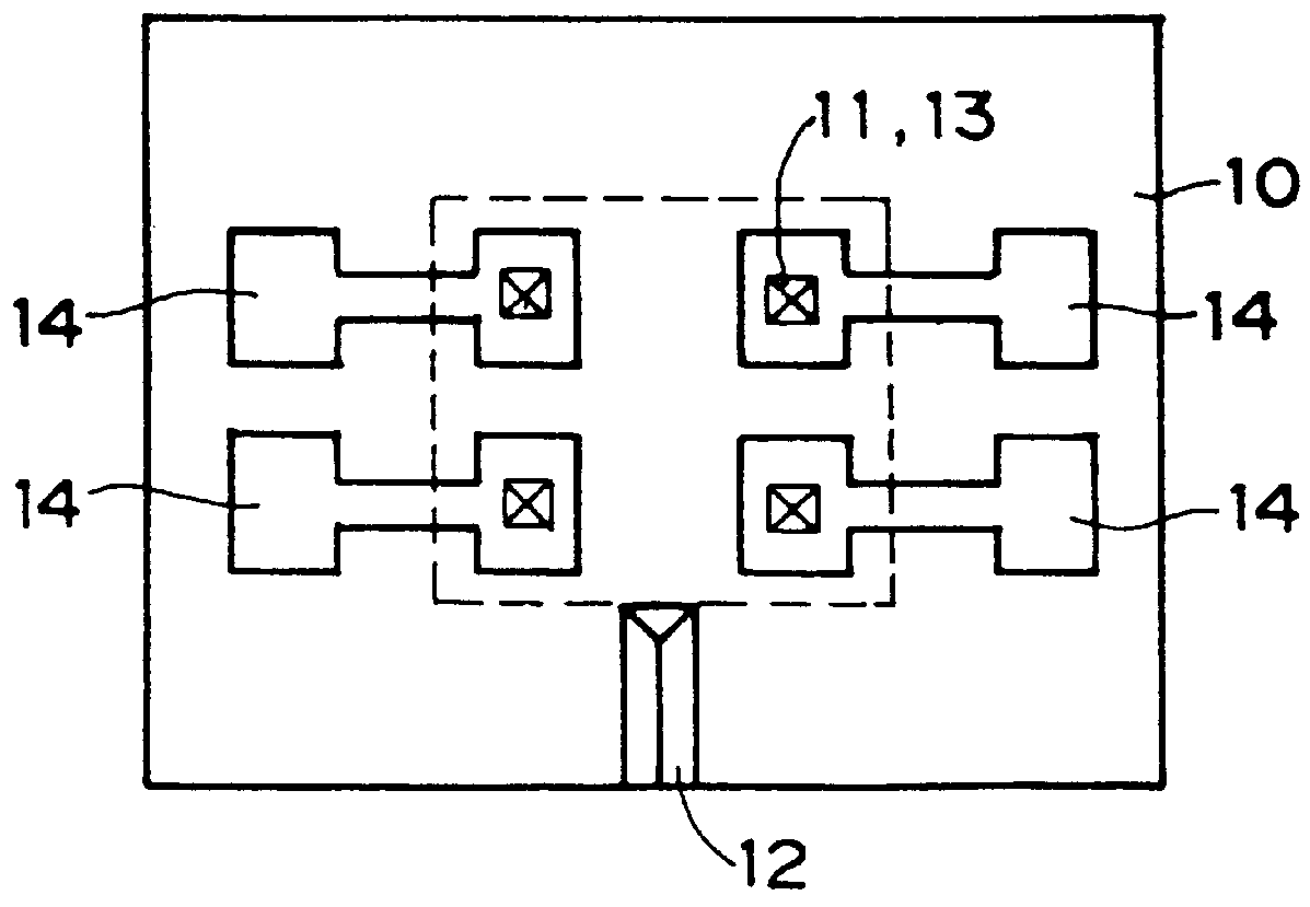
Referring to FIG. 4 for the third time, a supporting substrate (10) made of an Si plate of which the top surface is covered by an SiO.sub.2 film (not shown) is provided with at least two recesses (four recesses in the drawing) (11) and a V-groove (12) horizontally extending along the top surface of the Si plate to receive an optical fiber (not shown). The interna...

third embodiment

A method for mounting an optical semiconductor device having electrode patterns made of an Au--Sn alloy layer or a piled layer of Cr / Ni / Au or of Ti / Pt / Au and which is produced on the rear surface thereof, on a supporting substrate having recesses produced on the top surface thereof and being lined by electrode patterns made of an Au--Sn alloy layer or a piled layer of Cr / Ni / Au or of Ti / Pt / Au by connecting the electrode patterns each other employing a creamy solder, based on "the self alignment results", wherein the center of each of the electrode patterns made of an Au--Sn alloy layer or a piled layer of Cr / Ni / Au or of Ti / Pt / Au and which is produced on the rear surface of the optical semiconductor device deviates from the center of each of the recesses, whereby versatility is enhanced for the volume of the creamy solder to be fed into the recess, will now be discussed.

Referring to FIG. 4 for the fourth time, a supporting substrate (10) made of an Si plate of which the top surface is...


PUM


Abstract

Composite units of an optical semiconductor device and a supporting substrate are disclosed, in which the rear surface of the optical semiconductor device is provided with one or more electrode patterns and the top surface of the supporting substrate is provided with one or more electrode patterns. The optical semiconductor device and the supporting substrate are fixed to each other by once melting and solidifying one or more solder bumps which intervene between the one or more electrode patterns provided on the rear surface of the optical semiconductor device and the one or more electrode patterns provided on the top surface of the supporting substrate. A good grade of accuracy in the mutual geometric position of the optical semiconductor device and the supporting substrate is obtained in a horizontal direction due to a phenomenon called "the self alignment results" in this specification, in which a molten metal is inclined to become a ball based on surface tension. Methods for mounting an optical semiconductor device on a supporting substrate with a good grade of accuracy in the mutual geometric position therebetween in the horizontal direction, based on the same technical principle, are also disclosed. To realize the foregoing results, each of the composite units of an optical semiconductor device and supporting substrate in accordance with this invention is given various structures specific to each of them, and each of the methods in accordance with this invention is given various steps or processes specific to each of them.

Description

This invention relates to a variety of improvements applicable to a composite unit of an optical semiconductor device and a supporting substrate and to a variety of improvements applicable to a method for mounting an optical semiconductor device on a supporting substrate.An optical fiber may be employed to transmit an optical signal emitted by a light emitting diode or a laser diode and / or an optical signal received by a photo diode. Accordingly, connection of an optical fiber and an optical semiconductor device, e.g. a light emitting diode a laser diode or a photo diode, is an important parameter in the technical field of optical signal transmission. In this sense, development of a device employable for coupling or uncoupling an optical fiber and an optical semiconductor device is a long standing subject to enhance the optical signal transmission technology and to cause the optical signal transmission technology to prevail in society.The requirements for such a device include the f...

Claims


Application Information

Patent Timeline
IPC IPC(8): H01L31/0203H01L33/00H01L33/38H01L33/62
CPCH01L31/0203H01L33/62H01L2224/16H01L23/48H01L21/60
Inventor MATSUKURA, HISAOKUDOU, YASUHIKOHOTTA, HAJIMEHIRAKAWA, AKIOSUGAWARA, MASAKIUTSUNOMIYA, JIROKUROSAWA, KIYOSHI
Owner NEOPHOTONICS SEMICON GK
Why Eureka
Try Eureka