Photomask blank, photomask, and methods of manufacturing the same

a technology of photomask and resist film, which is applied in the field of photomask blank, photomask and method of manufacturing the same, can solve the problems of difficult to completely suppress oxidation, adversely affecting optical properties, and inability to achieve substantial dry etching with chlorine-based gas, so as to achieve high light shielding properties and reduce the consumption of resist film during dry etching

Active Publication Date: 2009-08-27
HOYA CORP
View PDF7 Cites 16 Cited by
  • Summary
  • Abstract
  • Description
  • Claims
  • Application Information

AI Technical Summary

Benefits of technology

[0010]Ta has started to be paid attention to as a material having high light-shielding properties than Cr in exposure by an ArF excimer laser (wavelength: 193 nm) (hereinafter referred to as “ArF exposure”) and being dry-etchable with an etching gas containing substantially no oxygen gas. Ta metal or Ta compound other than Ta oxide has an advantage of being dry-etchable only with a chlorine-based gas or a fluorine-based gas. Even in the case of Ta oxide, although substantial dry etching cannot be achieved with a chlorine-based gas because the etching rate is very low, substantial dry etching can be achieved wi...

Problems solved by technology

Even in the case of Ta oxide, although substantial dry etching cannot be achieved with a chlorine-based gas because the etching rate is very low, substantial dry etching can be achieved with a fluorine-based gas.
However, Ta metal is a material that is very easily oxidized in the atmosphere and, thus, if this is used as a light-shielding film, there arises a problem.
Therefore, in the case where a photomask blank is fabricated by forming a Ta oxide light-shielding film on a transparent substrate of quartz glass widely used in photomask blanks for ArF exposure, there has been a problem that when a resist film is coated on the light-shielding film and then formed with a transfer pattern by EB writing or the like and then the Ta oxide light-shielding film is dry-etched with a fluorine-based gas using the patterned resist film as a mask, a pattern is accurately transferred into the Ta oxide light-shielding film, but the transparent substrate is also dry-etched with the fluorine-based gas or the surface of the transparent...

Method used


Image

  • Photomask blank, photomask, and methods of manufacturing the same
  • Photomask blank, photomask, and methods of manufacturing the same
  • Photomask blank, photomask, and methods of manufacturing the same

Examples


example 1

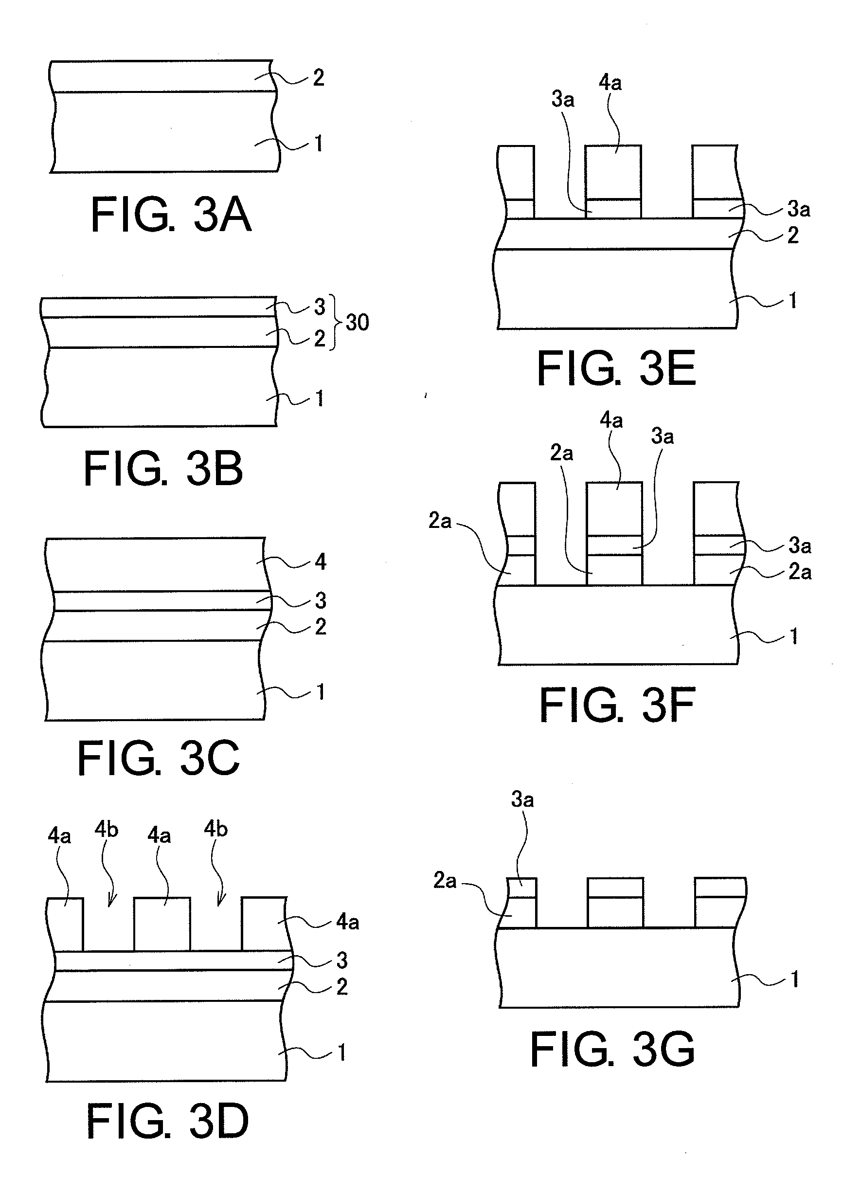
[0043]A substrate 1 made of synthetic quartz and having an about 152 mm×152 mm square size with a thickness of 6.35 mm was introduced into a DC magnetron sputtering apparatus. After the inside of the sputtering apparatus was evacuated to 2×10⁻⁵ (Pa) or less, a mixed gas (sputtering gas) of Xe and N2 was introduced into the sputtering apparatus. In this event, the flow rate of Xe and the flow rate of N2 were adjusted to 11 sccm and 15 sccm, respectively. Ta was used as a sputtering target. After the gas flow rates were stabilized, the power of a DC power supply was set to 1.5 kW, thereby forming a Ta nitride layer 2 having a thickness of 44.9 nm on the substrate 1 (see FIG. 3A).

[0044]Then, while the substrate 1 formed with the Ta nitride layer 2 was maintained in the sputtering apparatus, a mixed gas (sputtering gas) containing an Ar gas at a flow rate of 58 sccm and an O2 gas at a flow rate of 32.5 sccm was introduced into the sputtering apparatus and then the power of the DC power ...

example 2

[0062]FIG. 4 is a sectional view illustrating the structure of a photomask blank according to Example 2. As shown in FIG. 4, the photomask blank according to Example 2 is configured such that a Ta—B—N layer 21 having a thickness of 46.7 nm is formed as a light-shielding layer on a glass substrate 1 made of synthetic quartz and a Ta—B—O layer 31 having a thickness of 10 nm is formed as a front-surface antireflection layer on the Ta—B—N layer 21. The Ta—B—N layer 21 and the Ta—B—O layer 31 form a light-shielding film 33. Herein, the N content of the Ta—B—N layer 21 is 15 at % and the 0 content of the Ta—B—O layer 31 is 58 at %.

[0063]The photomask blank according to Example 2 is manufactured in the following manner: As in Example 1, a substrate 1 made of synthetic quartz and having an about 152 mm×152 mm square size with a thickness of 6.35 mm was introduced into a DC magnetron sputtering apparatus. After the inside of the sputtering apparatus was evacuated to 2×10⁻⁵ (Pa) or less, a mi...

example 3

[0070]FIG. 5 is a sectional view illustrating the structure of a reflective photomask blank according to Example 3. The reflective photomask blank is a photomask blank for fabricating a reflective photomask particularly for use in extreme ultraviolet (EUV) lithography using EUV light (wavelength: about 13 nm). The reflective photomask blank is formed by stacking a multilayer reflective film 11, an intermediate film 12, and an absorbent film (light-shielding film) 13 in this order on a substrate 10. The multilayer reflective film 11 is a film adapted to reflect EUV light with high reflectance and normally has a structure in which a material having a relatively high refractive index and a material having a relatively low refractive index are alternately layered in the order of several nm. As the multilayer reflective film 11, use is widely made of a Mo / Si cycle multilayer reflective film in which Mo and Si are alternately layered by approximately 40 cycles. As examples of other multil...


PUM

PropertyMeasurementUnit
Fractionaaaaaaaaaa
Fractionaaaaaaaaaa
Fractionaaaaaaaaaa

Abstract

A photomask blank has a light-shielding film composed of at least two layers on a transparent substrate. The light-shielding film includes a light-shielding layer made of a material mainly containing tantalum nitride and further containing xenon and a front-surface antireflection layer formed on the light-shielding layer and made of a material mainly containing tantalum oxide and further containing argon.

Description

[0001]This application is based on and claims the benefit of priority from Japanese Patent Application No. 2008-046890, filed on Feb. 27, 2008, and Japanese Patent Application No. 2009-015734, filed on Jan. 27, 2009, the disclosures of which are incorporated herein in their entirety by reference.TECHNICAL FIELD[0002]This invention relates to a photomask blank for use as an intermediate product in manufacturing a photomask for use as a mask in, for example, transferring a fine pattern in the manufacture of semiconductor devices and to the photomask and further relates to methods of manufacturing them.BACKGROUND ART[0003]Generally, in the manufacture of semiconductor devices or the like, a fine pattern is formed by photolithography and, in a fine pattern transfer process where the photolithography is performed, a photomask is used as a mask. The photomask is generally obtained by forming a desired fine pattern in a light-shielding film or the like of a photomask blank as an intermedia...

Claims


Application Information

Patent Timeline
IPC IPC(8): G03F1/00C23C14/06G03F1/50G03F1/54G03F1/58
CPCG03F1/58G03F1/46G03F1/54G03F1/66H01L21/0276H01L21/0337H01L21/2033H01L21/2036
Inventor NOZAWA, OSAMU
Owner HOYA CORP
Why Eureka
Try Eureka