Integrated circuit having surge protection circuit

a technology of integrated circuits and surge protection circuits, which is applied in the field can solve the problems of heat dissipation effect of semiconductor integrated circuits, failure of output transistors, and inability to meet the requirements of the circuit,

Inactive Publication Date: 2000-07-11
NISSAN MOTOR CO LTD
View PDF8 Cites 88 Cited by
  • Summary
  • Abstract
  • Description
  • Claims
  • Application Information

AI Technical Summary

Problems solved by technology

The back electromotive voltage induced by turning off the current in the inductive load can cause breakdown of the output transistor, since the output transistor is in a high impedance state.
When a solenoid is used as the load of the output transistor, a back electromotive voltage induced by a process of turning the solenoid off is becoming a problem.
However, when the feature size of the semiconductor integrated circuit is minimized, and the chip size becomes smaller and smaller, a heat dissipation effect of the semiconductor integrated circuit will inevitably shrink.
Since the heat generated by a semiconductor element is transported away from the chip surface to a heat sink through material such as adhesives, a decrease of the heat dissipation effect results in thermal runaway of the device.
In particular, generation of heat at the output stage of a power semiconductor element whose power loss is large is one of the factors interfering with chip size reduction of the semiconductor integrated circuit.
Therefore, the chip size-reduction of the conventional semiconductor integrated circuit is hindered.

Method used


Image

  • Integrated circuit having surge protection circuit
  • Integrated circuit having surge protection circuit
  • Integrated circuit having surge protection circuit

Examples


first embodiment

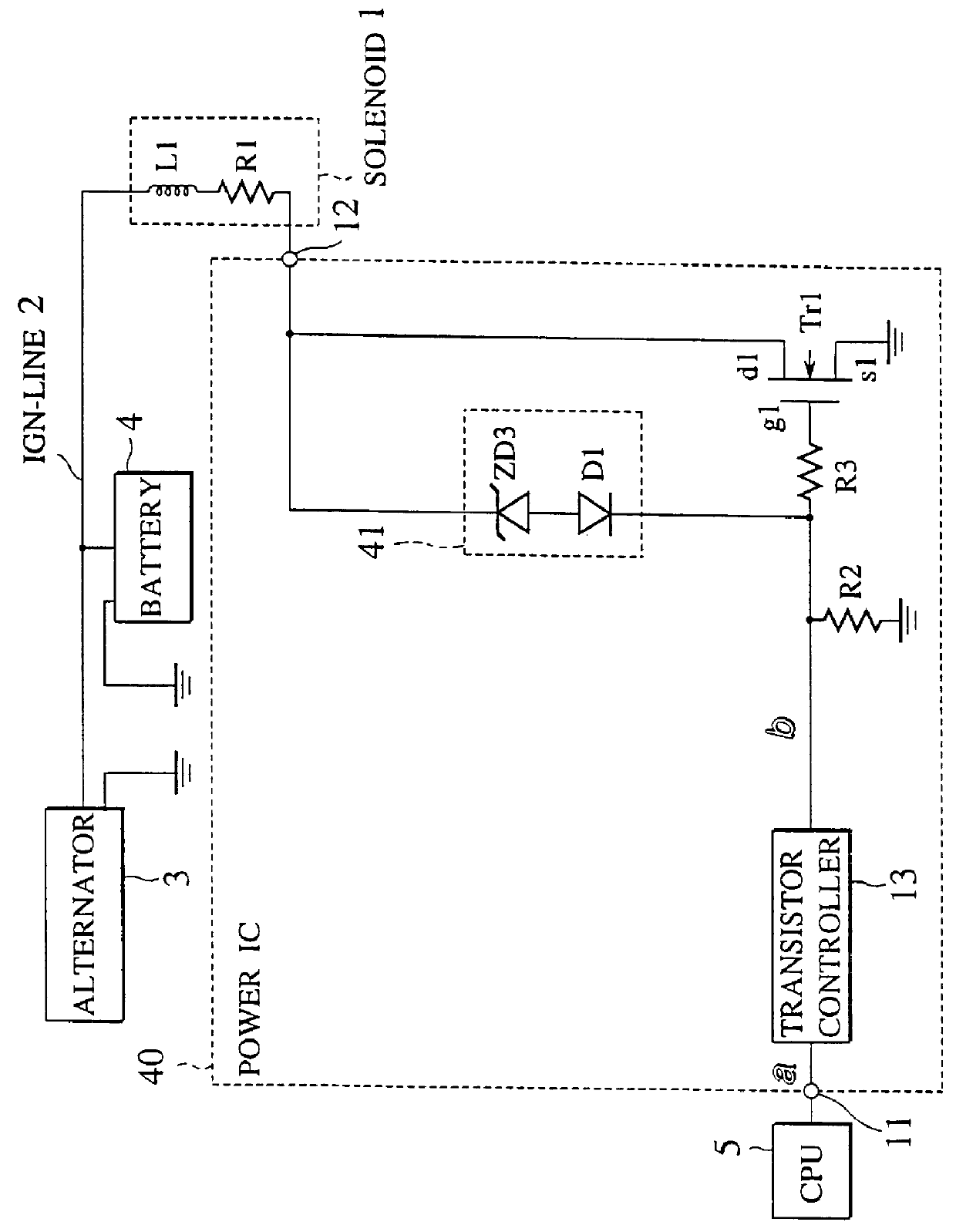
That is, the power IC 10 according to the present invention mounts a semiconductor element controller (hereinafter referred to as "a transistor controller") 13 controlling the on / off-states of the output transistor Tr1; a clamping circuit 14 for protecting the output transistor Tr1; and the clamp controlling circuit 15, or the like, on the same chip with the output transistor Tr1. The clamping circuit 14 is a circuit for protecting the output transistor Tr1 from the surge voltage being supplied through the output terminal 12 and is constituted by "an overvoltage protection element" conducting over the given voltage. As the overvoltage protection element, the Zener diode is preferable. Specifically, as shown in FIG. 5, the clamping circuit 14 is constituted by a diode D1 and a Zener diode ZD1 connected in series with their respective anode sides joined together.

An inductive load 1 is connected to the drain D1 of the output transistor Tr1. The solenoid 1, as this inductive load, compr...

second embodiment

As shown in FIG. 9, a semiconductor integrated circuit (a power IC) 20 according to a second embodiment of the present invention mounts a semiconductor element controller (a transistor controller) 13; a clamping circuit 14; and a clamp controlling circuit 21, or the like, on the same chip with the output semiconductor element (an output transistor Tr1). In the second embodiment of the present invention, the constitution of the clamp controlling circuit 21 differs from the first embodiment of the present invention.

That is, the clamp controlling circuit 21 according to a second embodiment of the present invention is constituted by an output voltage monitor 22; an edge detector 23; and a timer 24 as shown in FIG. 9. Furthermore, the clamp controlling circuit 21 comprises a switching element Tr2 connected between the output terminal 12 and the clamping circuit 14. The output voltage monitor 22 is constituted by a reference voltage generator 25 sending a reference voltage; a first resist...

third embodiment

As shown in FIG. 11, a semiconductor integrated circuit (a power IC) 30 according to a third embodiment of the present invention mounts a semiconductor element controller (a transistor controller) 13; a clamping circuit 31; and a clamp controlling circuit 21, or the like, on the same chip with the output semiconductor element (an output transistor Tr1). In the third embodiment of the present invention, the constitution of the clamp controlling circuit 31 differs from the first and the second embodiments of the present invention. The third embodiment of the present invention is the same as the second embodiment in the point that the clamp controlling circuit 21 is constituted by an output voltage monitor 22, an edge detector 23, a timer 24 and the switching element Tr2.

As shown in FIG. 11, a clamping circuit 31 of a power IC 30 according to a third embodiment of the present invention is constituted by a diode D1; a first overvoltage protection element (a Zener diode) ZD1; and a secon...


PUM


Abstract

A trailing edge of a control signal of a transistor controller for controlling an output transistor is detected by an edge detector of a clamp controlling circuit. A surge voltage from a back electromotive voltage induced in an inductance L1 is absorbed from the output transistor, only for a given period immediately after the solenoid is turned off, by turning a switching transistor into an on-state by a timer to force a clamping circuit into conduction. At a normal operation, since the clamping circuit is cut off from an output terminal, the clamping voltage can be set in a manner to reduce to a normal voltage in an IGN-line. Therefore, a peak power value of a power loss caused by the surge voltage at the output transistor can be reduced, whereby generation of heat at the output transistor can be reduced. Therefore, the chip size of the power IC can be reduced.

Description

1. Field of the InventionThis invention relates to a semiconductor integrated circuit having an active clamping circuit for protecting a semiconductor element at an output stage from an overvoltage applied externally.2. Description of the Related ArtA power IC having a transistor at the output stage (hereinafter referred to as "an output transistor"), a driving circuit and / or a controlling circuit for the transistor, and a protection circuit for the transistor, integrated on the same chip, is well known.It is frequently the case that, a high voltage due to static electricity, a surge voltage induced in an induction load and, irregularity of the load, is supplied to an output terminal of this output transistor as an overvoltage. Therefore, various overvoltage protection circuits protecting the output transistor from these overvoltages have been devisedIn recent years, the switching speed of the output transistor has become higher and higher. At a turn-off transition of the output tra...

Claims


Application Information

Patent Timeline
Patent Type & Authority Patents(United States)
IPC IPC(8): H03K5/08H03K17/082H01L21/822H01L27/04H02H7/20H02H9/04H03F1/52
CPCH03K5/08H03K17/0822
Inventor GONDA, TOMOHIKOKIYOTA, SHIGEYUKI
Owner NISSAN MOTOR CO LTD
Why Eureka
Try Eureka