

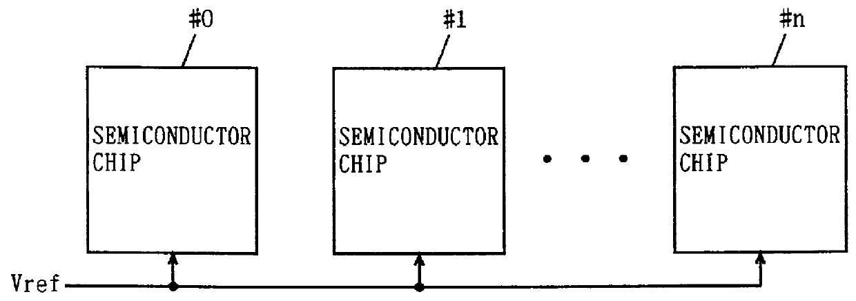
Semiconductor device allowing fast and stable transmission of signals
a semiconductor and signal technology, applied in the field of output circuits, can solve the problems of increasing current consumption, increasing power consumption, and limited fan-out at the output circui
- Summary
- Abstract
- Description
- Claims
- Application Information
AI Technical Summary
Problems solved by technology
Method used
Image

Examples
Embodiment Construction
]
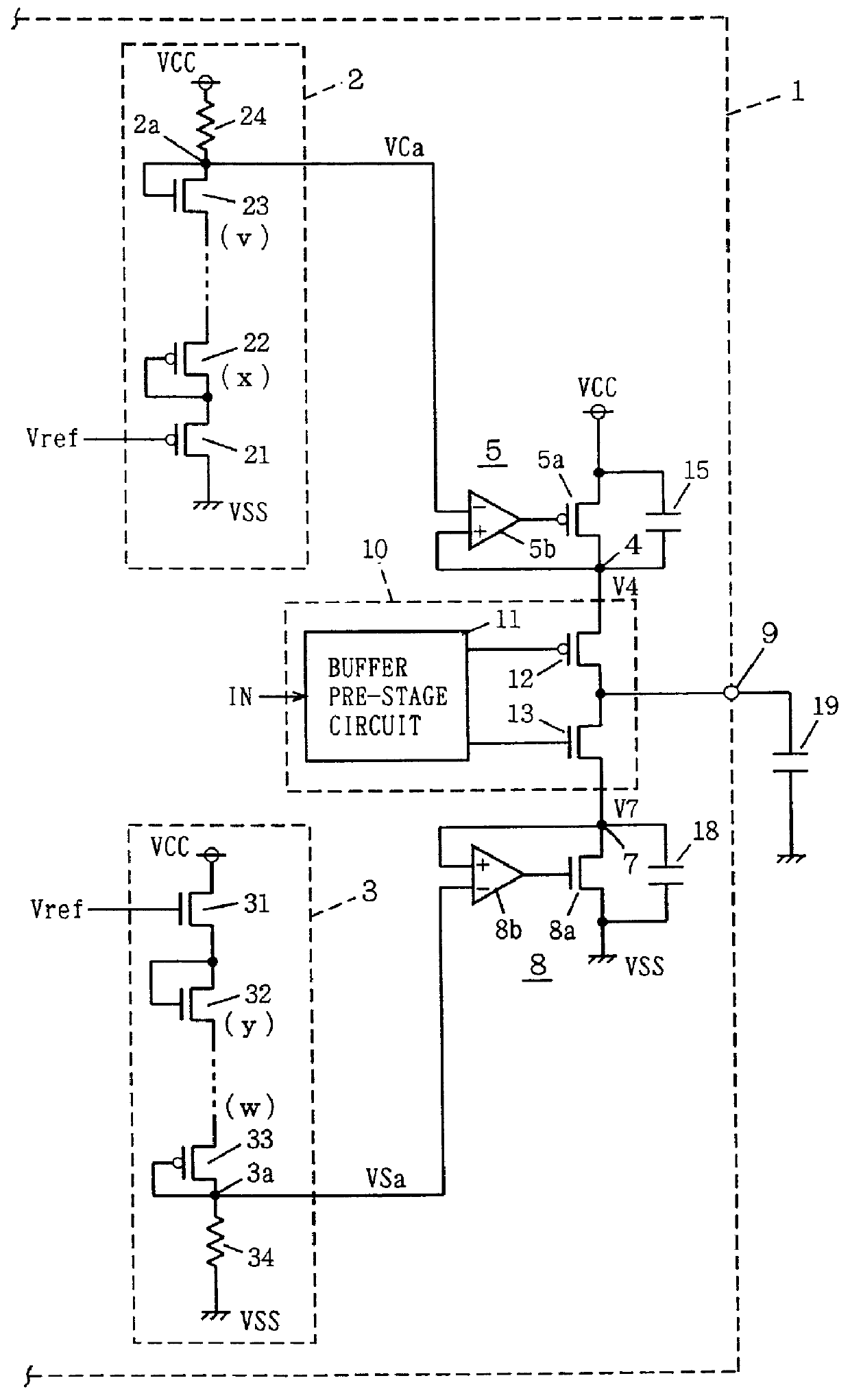
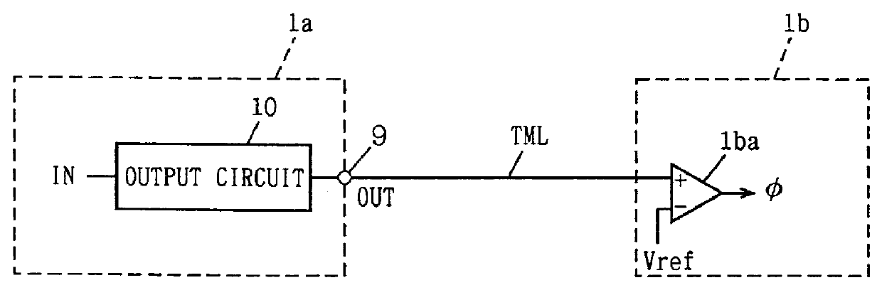
The invention may be used in a system including a terminating resistance arranged on a transmission line. A driving capability of a transistor in an output stage can be increased independently of a residence value of this terminating resistance so that a system allowing fast operation can be implemented.
As described above, the invention can provide a semiconductor integrated circuit which can stably produce the internal power supply voltage at a predetermined voltage level according to the reference voltage, and can operate stably and fast.
Although the present invention has been described and illustrated in detail, it is clearly understood that the same is by way of illustration and example only and is not to be taken by way of limitation, the spirit and scope of the present invention being limited only by the terms of the appended claims.
PUM
 Abstract
Description
Claims
Application Information