External cavity laser

a laser and cavity technology, applied in the direction of instruments, semiconductor lasers, semiconductor laser structural details, etc., can solve the problems of difficult integration of temperature controllers, inability to accurately control output wavelengths from wafer to wafer, and complicated device temperature stabilisation

Inactive Publication Date: 2000-08-08
KOTURA
View PDF1 Cites 159 Cited by
  • Summary
  • Abstract
  • Description
  • Claims
  • Application Information

AI Technical Summary

Benefits of technology

Also, as the grating is separate from the active region of the laser, ageing has no effect on the output wavelength with the result that compensated drive circuits are also not required.
The combination of these factors makes possible a single chip solution to control both temperature stabilisation an

Problems solved by technology

DFB lasers have a major disadvantage in that, since the output wavelength is a function of both the grating period and the effective refractive index of the device, the output wavelength cannot be accurately controlled from wafer to wafer.
This tuning requirement complicates the temperature stabilisation of the devices, as components such as variable value resistors must be included, making an integrated temperature controller difficult.
DBR lasers suffer from similar problems (i.e. changes in effective index and variations in the grating period), with the added difficulty that, due to production tolerances, the relative grating phases of the two Bragg reflectors become unpredictable, resulting in low production yields, or a requirement for a phase adjustment region.
In general DBR lasers are more complex and more difficult to manufacture than DFBs

Method used


Image

  • External cavity laser
  • External cavity laser
  • External cavity laser

Examples


Embodiment Construction

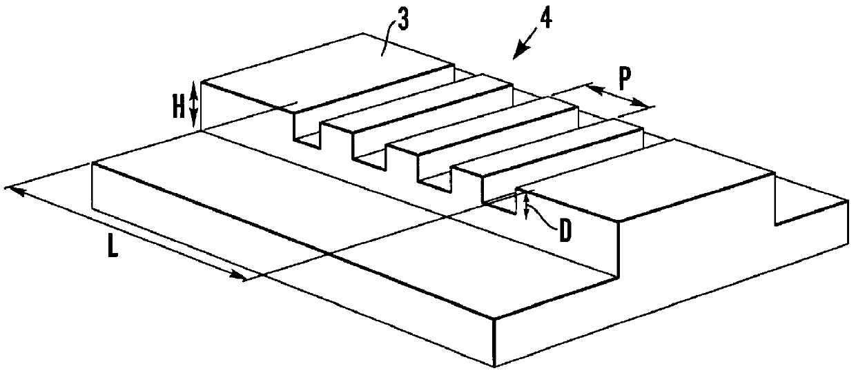
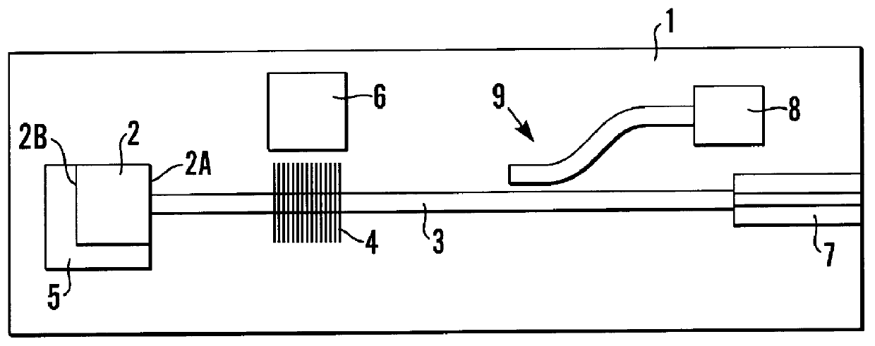
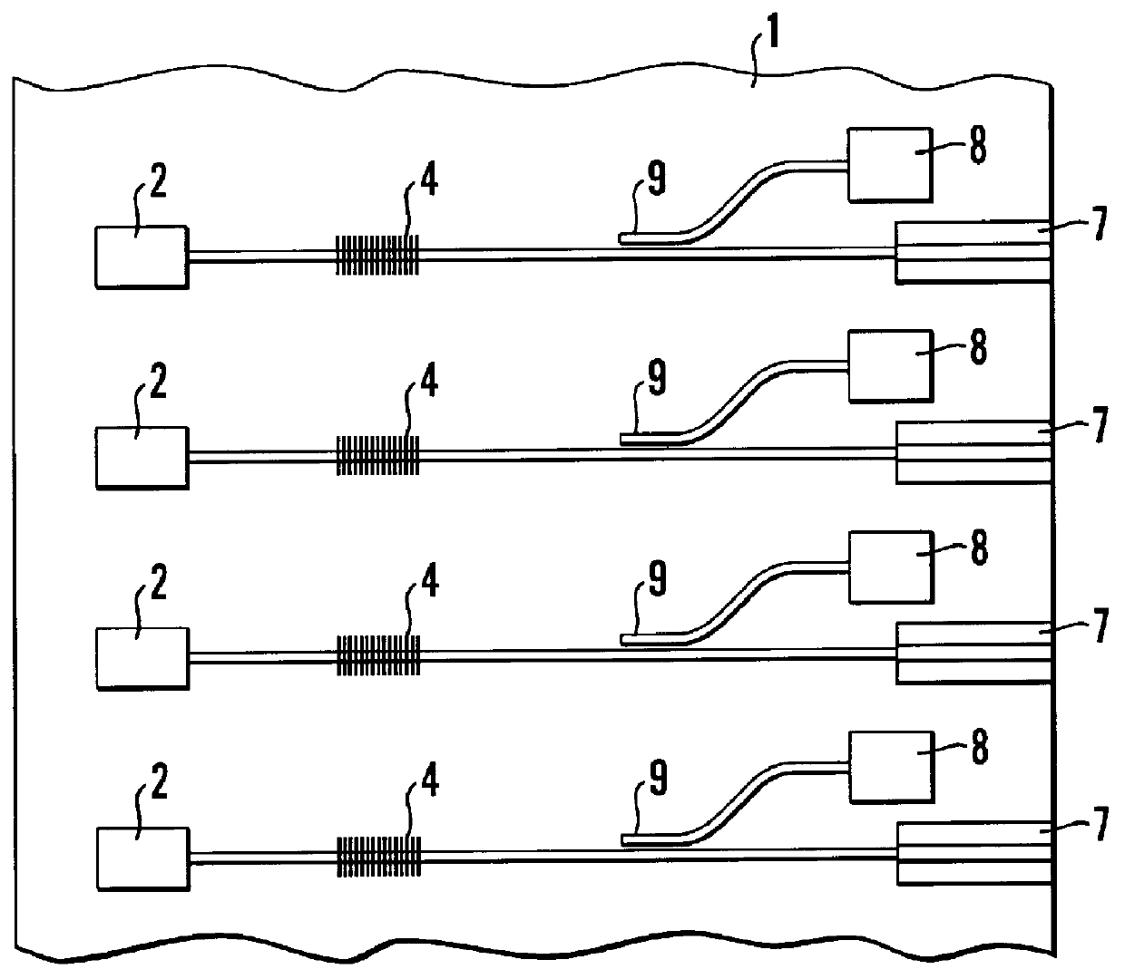
FIG. 1 shows an external cavity laser formed on an SOI chip 1 which comprises an upper, light transmissive layer of silicon separated from a silicon substrate by an insulating layer, typically of silicon dioxide. The device comprises an RA 2, aligned with a silicon waveguide 3 in which a grating 4 is provided.

The RA preferably includes a waveguide therein at an angle to the normal of its front facet 2A. A back facet 2B of the RA is coated with a HR coating and the front facet thereof is AR coated.

The RA 2 is passively aligned on the SOI chip 1 by means of location surfaces of the RA being abutted against location surfaces of a location recess 5 etched in the SOI chip 1. Further details of this method of mounting an optical component are given in U.S. application Ser. No. 08 / 853,104; the disclosure of which is incorporated herein by reference.

The RA 2 is coupled to the silicon waveguide 3 within which a Bragg grating 4 is formed. The grating 4 effectively forms the front facet of the...


PUM


Abstract

External Cavity Laser An external cavity laser comprising first and second feedback means with an optical gain medium (2) therebetween, one of the feedback means is provided by a grating (4) formed in a silicon waveguide and the other feedback means is provided by a reflective back facet (2B) of the optical gain medium (2). The output wavelength of the laser, at a given temperature, can thus be determined during its manufacture and the laser can be made by mass production techniques. The grating (4) may be thermally isolated to obviate the need for temperature control means (6) to control the temperature of the grating (4). An array of lasers may be provided on a single chip.

Description

This invention relates to external cavity lasers, particularly narrow linewidth lasers for use in telecommunication applications.Several methods exist for constructing narrow linewidth single mode semi conductor lasers. Practical devices fall into two groups, monolithic semiconductor devices, and external cavity lasers. All of these use frequency selective feedback to achieve single mode operation over a range of drive currents.Frequency selective feedback may be provided by a periodic structure either with an external element or within the semiconductor (i.e. monolithic), which can take the form of a DBR (distributed Bragg reflector) or DFB (distributed feedback) laser. In a DBR the grating is outside the active region but in the monolithic semiconductor, whereas the grating in DFB lasers is within the active region. External cavity lasers consist of an optical gain medium that is located between, but does not occupy the full distance between, two reflectors, one reflector commonly...

Claims


Application Information

Patent Timeline
IPC IPC(8): H01S5/00H01S5/026H01S5/40H01S5/02H01S5/14H01S5/022
CPCH01S5/02248H01S5/02284H01S5/0683H01S5/141H01S5/4031H01S5/4087H01S5/02325H01S5/02251H01S5/02415H01S5/06256H01S5/0262H01S5/0422H05B3/12
Inventor BESTWICK, TIMOTHY DAVIDTIDMARSH, JOLYON RICHARDFASHAM, STEPHEN JAMES
Owner KOTURA
Why Eureka
Try Eureka