Method of making semiconductor devices having protruding contacts

Inactive Publication Date: 2000-08-22
PANASONIC CORP
View PDF13 Cites 18 Cited by
  • Summary
  • Abstract
  • Description
  • Claims
  • Application Information

AI Technical Summary

Benefits of technology

A method for manufacturing semiconductor devices according to the present invention comprises the steps of aligning a protruding contact on a first semiconductor device with an electrode on a second semiconductor device or a circuit board; applying an insulating resin containing a reducing agent to a protruding contact on the first semiconductor device and/or an electrode of the second semiconductor device or the circuit board; and hardening the insulating resin.
A method for manufacturing semiconductor devices in accordance with the present invention comprises the steps of forming first and second protruding contacts having different hardnesses respectively on a first semiconductor chip and a second semiconductor chip or a circuit board; aligning said fi

Problems solved by technology

Accordingly, the prior art process is complex.
Furthermore, it is difficult in the above described manufacturing process to provide protruding contacts 15 at a fine pitch.
This fact limits the possibility of manufact

Method used


Image

  • Method of making semiconductor devices having protruding contacts
  • Method of making semiconductor devices having protruding contacts
  • Method of making semiconductor devices having protruding contacts

Examples


Example

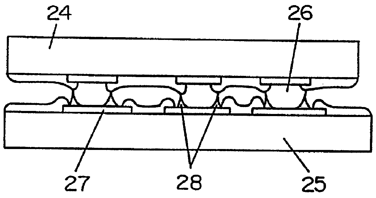
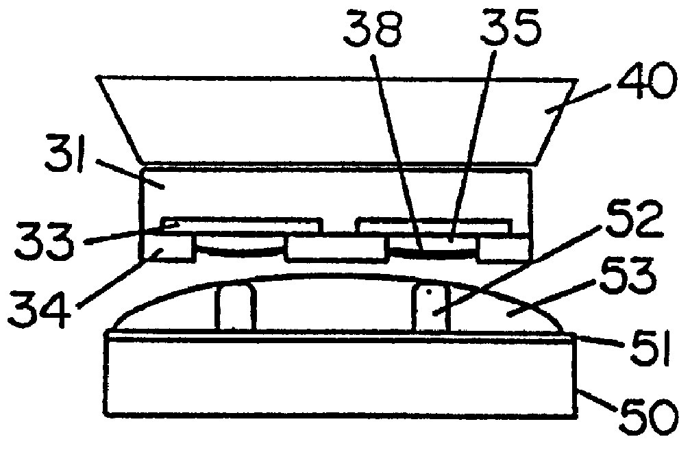
FIG. 3 shows a cross sectional view of a semiconductor device according to a preferred embodiment of the present invention. Provided inside a semiconductor chip 31 is an active layer 32 comprising transistors, wirings, contacts, or like structures. On the active surface of semiconductor chip 31, chip electrodes 33 such as Al electrodes are formed at intervals of approximately 30 .mu.m. The chip electrode of the present embodiment comprises an Al material, containing about 0.5% Cu, having a thickness of approximately 0.6 .mu.m. The main material for chip electrode 31, however, is not limited to Al, but the chip electrode may comprise a material containing Cu as the principal ingredient.

Formed on the active surface of semiconductor chip 31 is a protection layer 34, which is a silicon nitride film approximately 0.8 .mu.m thick. The protection layer 34 is provided with openings each having a 15 .mu.m inner diameter disposed at appropriate intervals for exposing the chip electrodes 33 of...


PUM


Abstract

A method of making semiconductor devices with contacts protruding from openings in a passivation layer over an active chip area. Inside each opening, a relatively hard barrier layer is provided and a flash-plated film is applied to subsequently form a relatively soft diffusion barrier layer when a protruding contact is formed. Two semiconductor devices with electrodes are joined by embedding relatively hard electrodes of a first device into relatively soft electrodes of a second device. A reducing agent can be incorporated into an insulating resin applied between semiconductor chips at areas other than the bonded electrodes.

Description

The present invention is directed to semiconductor devices in general, and in particular to semiconductor devices having protruding contacts for coupling those semiconductor devices with substrate electrodes of other semiconductor devices or circuit boards. The present invention is also directed to a method for manufacturing such semiconductor devices.Known methods for coupling together two semiconductor devices or a semiconductor device and a circuit board include the tape automated bonding (TAB) method, and flip chip method. The circuit board in this context may include, in addition to printed circuit boards comprising an insulating base board and an electro-conductive substrate electrode, thin film transistor (TFT) elements, piezoelectric elements and any other electrical elements that may be coupled electrically with semiconductor devices.In the flip chip method, a semiconductor device to be mounted is provided with protruding contacts of solder(e.g., a tin and lead alloy), and ...

Claims


Application Information

Patent Timeline
IPC IPC(8): H01L21/02H01L21/56H01L21/60H01L23/48H01L23/485
CPCH01L21/563H01L24/29H01L24/13H01L24/75H01L24/83H01L24/11H01L2924/0001H01L2224/13022H01L2224/13099H01L2224/16225H01L2224/73203H01L2224/73204H01L2224/75H01L2224/7525H01L2224/75252H01L2224/75301H01L2224/75745H01L2224/83102H01L2224/83192H01L2224/83874H01L2224/92125H01L2924/01005H01L2924/01013H01L2924/01015H01L2924/01029H01L2924/01033H01L2924/01039H01L2924/01046H01L2924/01049H01L2924/0105H01L2924/01078H01L2924/01079H01L2924/01082H01L2924/09701H01L2924/01006H01L2924/014H01L2924/0132H01L2924/15787H01L2924/15788H01L2224/16145H01L2224/32145H01L2224/32225H01L2224/29109H01L2224/29111H01L2224/2919H01L2924/00013H01L2224/13144H01L2224/13155H01L2224/13609H01L2924/00014H01L2924/01028H01L2924/00012H01L2924/00H01L2924/00015H01L2224/13109H01L2224/29099H01L2224/81191H01L2224/81192H01L2224/81193H01L2224/73104H01L2224/05124H01L2224/05155H01L2224/05644H01L24/03H01L24/05H01L23/00H01L21/60
Inventor OHTSUKA, TAKASHIKAWAKITA, TETSUOMATSUMURA, KAZUHIKOFUJIMOTO, HIROAKI
Owner PANASONIC CORP
Why Eureka
Try Eureka