Thermal ink jet printhead with increased heater resistor control

a technology of heater resistor and printhead, which is applied in the direction of printing, electrical equipment, and semiconductor devices, can solve the problems of separating bulging ink, difficult to accurately control the resistance, and excess heat, so as to increase the latitude of energy input, control the heater resistance, and control the heater resistance

Inactive Publication Date: 2000-11-14
XEROX CORP
View PDF6 Cites 9 Cited by
  • Summary
  • Abstract
  • Description
  • Claims
  • Application Information

AI Technical Summary

Benefits of technology

When the excess heat is removed from the ink, the vapor bubble collapses on the resistor, because the heat generating current is no longer applied to the resistor. As the bubble begins to collapse, the ink still in the channel between the nozzle and bubble starts to move towards the collapsing bubble, causing a volumetric contraction of the ink at the nozzle and resulting in the separating of the bulging ink as an ink droplet. The acceleration of the ink out of the nozzle while the bubble is growing provides the momentum and velocity to expel the ink droplet towards a recording medium, such as paper, in a substantially straight-line direction. The entire bubble expansion and collapse cycle takes about 20 microseconds (.mu.s). The channel can be refired after 100 to 500 .mu.s minimum dwell time to enable the channel to be refilled and to enable the dynamic refilling factors to be somewhat dampened.
According to a first aspect of the invention, a fabrication process is disclosed which allows a thick polysilicon layer to be used for the gate region and heater contact region while a thinner polysilicon layer forms the heater center region. The thickness of the center region can be adjusted more accurately to control the heater resistance. Thus, the heater resistance is controlled by adjusting the thickness of the heater element center region rather than by the lightly doped ion implantation technique of the prior art. The fabrication process improvement described is economically attractive, since this two-layer polysilicon process can be implemented with the same number of photolithographic mask levels as the conventional two-implant polysilicon resistor process.
According to a second aspect of the invention, amorphous silicon is used for the center region instead of polysilicon. In the prior art device referenced above, the deposition rate is too low to permit utilization of amorphous silicon. Amorphous silicon provides a smoother heater surface, which increases the latitude of the energy input, and in time, increases the yield process. By decreasing the thickness of the heater center region, amorphous silicon becomes a viable option.

Problems solved by technology

As the bubble begins to collapse, the ink still in the channel between the nozzle and bubble starts to move towards the collapsing bubble, causing a volumetric contraction of the ink at the nozzle and resulting in the separating of the bulging ink as an ink droplet.
The more resistive the heaters, the lower the doping level, and the more difficult it is to accurately control the resistance.
When resistance is too low, threshold voltage is too low, and the extra voltage applied to the printhead results in excess heat, which causes ink to bake on the heater.
This results in an extra insulting layer on the heater, decreasing energy transferred to the ink, creating smaller drops and eventually completely failing to eject drops.
In addition, "over voltage" operation results in decreased heater lifetime.
In the prior art device referenced above, the deposition rate is too low to permit utilization of amorphous silicon.

Method used


Image

  • Thermal ink jet printhead with increased heater resistor control
  • Thermal ink jet printhead with increased heater resistor control
  • Thermal ink jet printhead with increased heater resistor control

Examples


Embodiment Construction

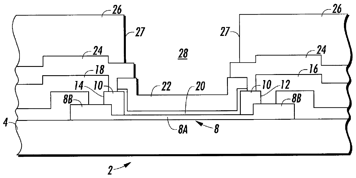
FIG. 1 is an enlarged, cross-sectional view of a heater element 2 fabricated according to the invention. Although only one heater element is illustrated, heater elements of the printheads are generally produced in large arrays of several hundred elements. When all of the resistors of the heater elements are fabricated concurrently, they will have substantially uniform sheet resistance, and the resistances between individual resistors of the heater elements in a printhead and from printhead to printhead will be substantially uniform.

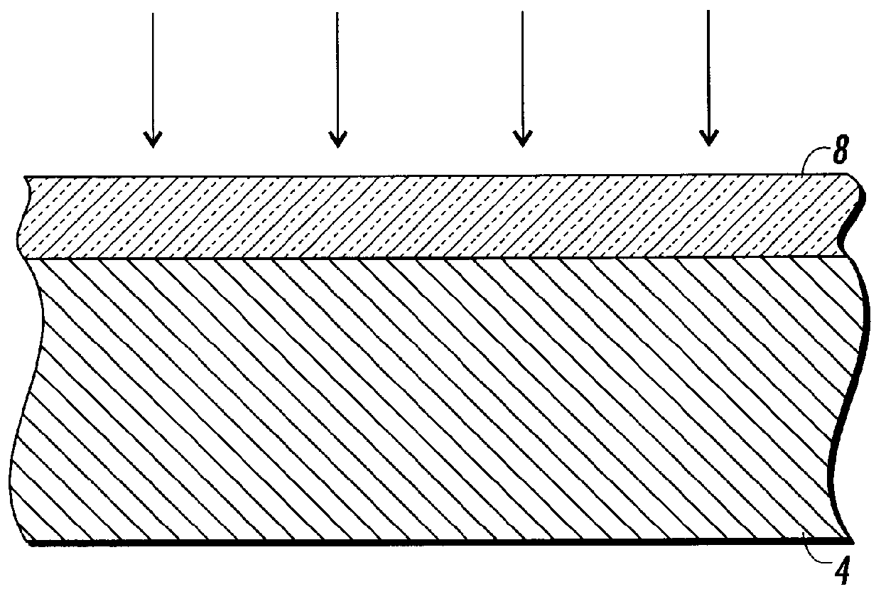
The heater element is formed by depositing polysilicon on top of substrate 4 and etching to form a resistor 8. The resistor 8 has a doped n-type region 8A which is thinner than two heavily doped n-type regions 8B formed at ends of region 8A. The process for forming regions 8A and 8B will be described below.

Phosphosilicate glass (PSG) is deposited and reflowed on top of the resistor 8 and etched to form the PSG step regions 10 which expose a top surface of...


PUM


Abstract

An improved method is disclosed for forming heater elements for an ink jet printhead. The resistance is more closely controlled by doping a central heater region which is formed relatively thinner than the heavily doped heater regions which are used as the gate and contact areas. The thinner central region can doped relatively heavy in order to more accurately adjust the heater resistance. In another embodiment, the thin layer is amorphous silicon rather than the polysilicon to increase the latitude of the energy input.

Description

BACKGROUND OF THE INVENTION AND MATERIAL DISCLOSURE STATEMENTThe present invention relates to thermal ink jet printers, and more particularly, to printheads incorporating a plurality of heater resistors which are selectively addressed to heat and expel ink from adjacent ink channels.Thermal ink jet printing utilizes printheads which use thermal energy to produce vapor bubbles in ink-filled channels to expel ink droplets. A thermal energy generator or heater element, usually a resistor, is located at a predetermined distance from a nozzle of each one of the channels. The resistors are individually addressed with an electrical pulse to generate heat which is transferred from the resistor to the ink.The transferred heat causes the ink to be super heated, i.e., far above the ink's normal boiling point. For example, a water based ink reaches a critical temperature of 280.degree. C. for bubble nucleation. The nucleated bubble or water vapor thermally isolates the ink from the heater eleme...

Claims


Application Information

Patent Timeline
Patent Type & Authority Patents(United States)
IPC IPC(8): B41J2/14B41J2/16
CPCB41J2/14129B41J2/1601B41J2/1628B41J2/1642B41J2/1631B41J2/1632B41J2/1629
Inventor BURKE, CATHIE J.RAISANEN, ALAN D.O'BRIEN, SEAN D.
Owner XEROX CORP
Why Eureka
Try Eureka