
Self-timed parallel data bus interface to direct storage devices

a data bus and direct storage technology, applied in error detection/correction, instruments, generating/distributing signals, etc., can solve the problems of limiting the useful length of parallel busses operating at high data rates, limiting the data rate of prior art busses comprised of parallel conductors, and changing the processor clock ra

Inactive Publication Date: 2001-02-20
IBM CORP
View PDF16 Cites 23 Cited by
  • Summary
  • Abstract
  • Description
  • Claims
  • Application Information

AI Technical Summary

Benefits of technology

Another object of the invention is the provision of a general purpose, low cost, high performance, point to point data communication link where the width and speed of the interface can easily be modified to tailor it to specific bandwidth requirements and to specific implementation technologies, including VLSI technologies.
Yet another object of the invention is to provide improved, cost-efficient attachment of direct access storage devices (DASD).
DASD I / O controllers can be based on redundant arrays of independent disks (RAID) technology. This significantly increases storage capacity per I / O controller, exceeding the access rate a single channel can support. Many channels are therefore needed per I / O controller. In lieu of using multiple (e.g., 10, 20) channels per I / O controller to match the increased I / O (DASD) controller capability, and still another object of this invention is to reduce the number of links required. A still further object of the invention is to enable channel commands, instead of being forwarded from system port to I / O sub-element channel function and then executed cooperatively by channel function and I / O (DASD) controller, to be forwarded through the I / O sub-element directly to the system DASD I / O controller for execution. Data associated with the commands is routed in the same manner.
Elimination of channel hardware reduces both total system size and cost providing a more effective means for the attachment of local DASD to computer systems.
Briefly, this invention contemplates the provision of a self-timed interface (STI) in which a clock signal clocks bit serial data onto a parallel, electrically conductive bus and the clock signal is transmitted on a separate line of the bus. The received data on each line of the bus is individually phase aligned with the clock signal. The received clock signal is used to define boundary edges of a data bit cell. It is defined individually for each line and the data on each line is individually phase adjusted so that, for example, a data transition position is in the center of the defined cell. The data is read into a buffer where it is decoded and read out synchronously with the receiver system clock. At the data rates contemplated in the application of this invention, the propagation delay is significant. However, within limits, the bus length is not critical and is independent of the transmit and received system clock. The phase adjustment can compensate for a skew of up to one bit cell across the width of the bus.

Problems solved by technology

As will be appreciated by those skilled in the art, such factors as noise and loading limit the useful length of parallel busses operating at high data rates.
Manufacturing tolerances associated with physical communication link (chips, cables, cord wiring, connectors, etc.) and temperature and variations in power supply voltage also limit the data rates on prior art busses comprised of parallel conductors.
Further, many prior art computer systems transfer data synchronously with respect to a processor clock, so that a change in processor clock rate may require a redesign of the data transfer bus.

Method used


Image

  • Self-timed parallel data bus interface to direct storage devices
  • Self-timed parallel data bus interface to direct storage devices
  • Self-timed parallel data bus interface to direct storage devices

Examples


Embodiment Construction

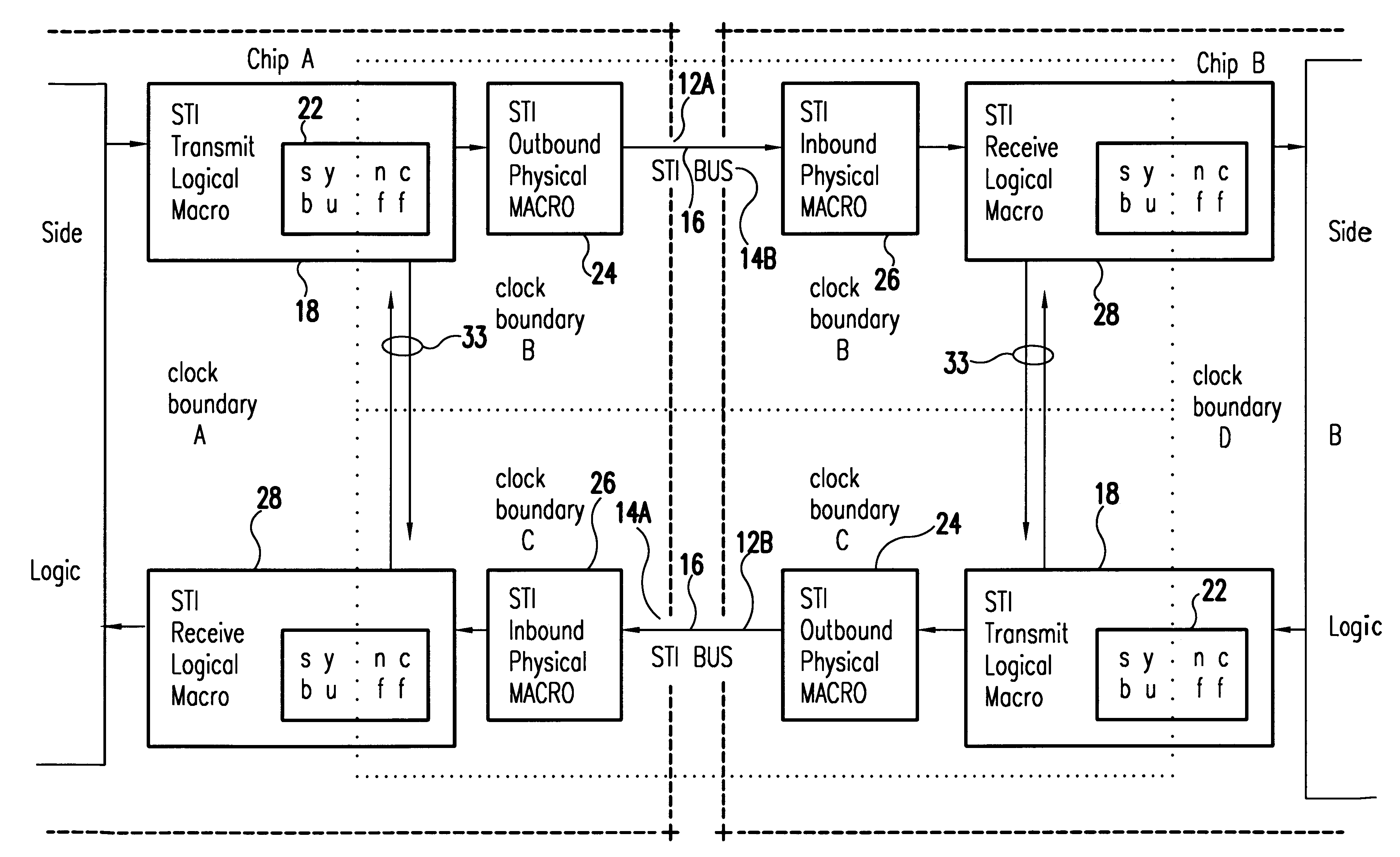
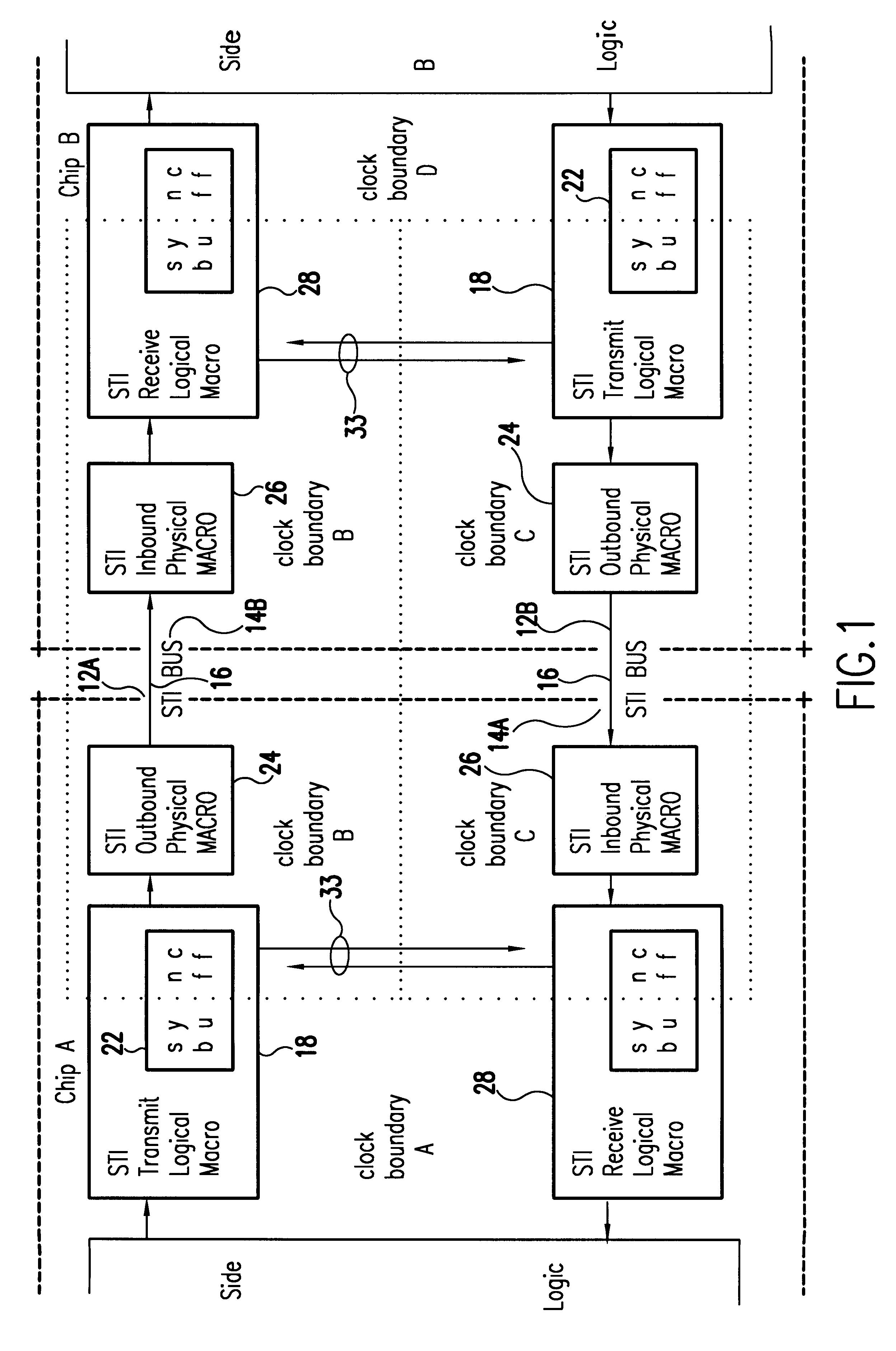
Referring now to FIG. 1 of the drawings, it illustrates one embodiment in which a self-timed interface in accordance with the teachings of this invention can be used. This exemplary embodiment of the self-timed interface provides data communications between two microprocessor chips, labeled here as Chip A and Chip B. However, as will be apparent to those skilled in the art, the self-timed interface of this invention is applicable to provide data transfer between a wide variety of components or nodes.

Chip A has a transmit port labeled 12A and Chip B has a transmit port labeled 12B. Similarly, Chips A and B have receive ports labeled 14A and 14B, respectively. The ports are connected by two self-timed interface busses 16; one for each transmission direction. In this exemplary embodiment of the invention, each bus 16 is one byte wide, and comprised of ten electrical conductors; nine conductors for data and one conductor for a clock signal.

Each transmit port (12A and 12B) includes a tra...


PUM


Abstract

An attached storage media link has a self-timed interface (STI) in which a clock signal clocks bit serial data onto a parallel, electrically conductive bus and the clock signal is transmitted on a separate line of the bus. The received data on each line of the bus is individually phase aligned with the clock signal, providing a high speed, cost effective interface to a direct access storage device.

Description

DESCRIPTION1. Field of the InventionThis invention relates to an improved method and apparatus for transmitting digital data at high speeds via a parallel data bus, and more particularly, to a method and apparatus that provides a cost effective interface to a direct access storage device.2. Description of the Prior ArtAs will be appreciated by those skilled in the art, such factors as noise and loading limit the useful length of parallel busses operating at high data rates. In the prior art, the length of the bus must be taken into account in the system design and the bus length must be precisely as specified. Manufacturing tolerances associated with physical communication link (chips, cables, cord wiring, connectors, etc.) and temperature and variations in power supply voltage also limit the data rates on prior art busses comprised of parallel conductors. Further, many prior art computer systems transfer data synchronously with respect to a processor clock, so that a change in proc...

Claims


Application Information

Patent Timeline
IPC IPC(8): G06F13/42G06F13/38
CPCG06F13/426
Inventor CASPER, DANIEL FRANCISBRADY, JAMES THOMASCAPOWSKI, ROBERT STANLEYCOX, FREDERICK JOHNFERRAIOLO, FRANK DAVIDHALMA, MARTEN JANWU, BENJAMIN HONG
Owner IBM CORP
Learn More