Seed layer structure for spin valve sensor

Inactive Publication Date: 2001-03-27
HITACHI GLOBAL STORAGE TECH NETHERLANDS BV
View PDF9 Cites 73 Cited by
  • Summary
  • Abstract
  • Description
  • Claims
  • Application Information

AI Technical Summary

Problems solved by technology

One of the disadvantages of the second class of materials, however, is that a read head employing a bottom pinning layer made of one of the second class of materials has a lower magnetoresistive coefficient (dr/R) than a read head having a pinning layer made f

Method used


Image

  • Seed layer structure for spin valve sensor
  • Seed layer structure for spin valve sensor
  • Seed layer structure for spin valve sensor

Examples


example 2

First Embodiment of Invention

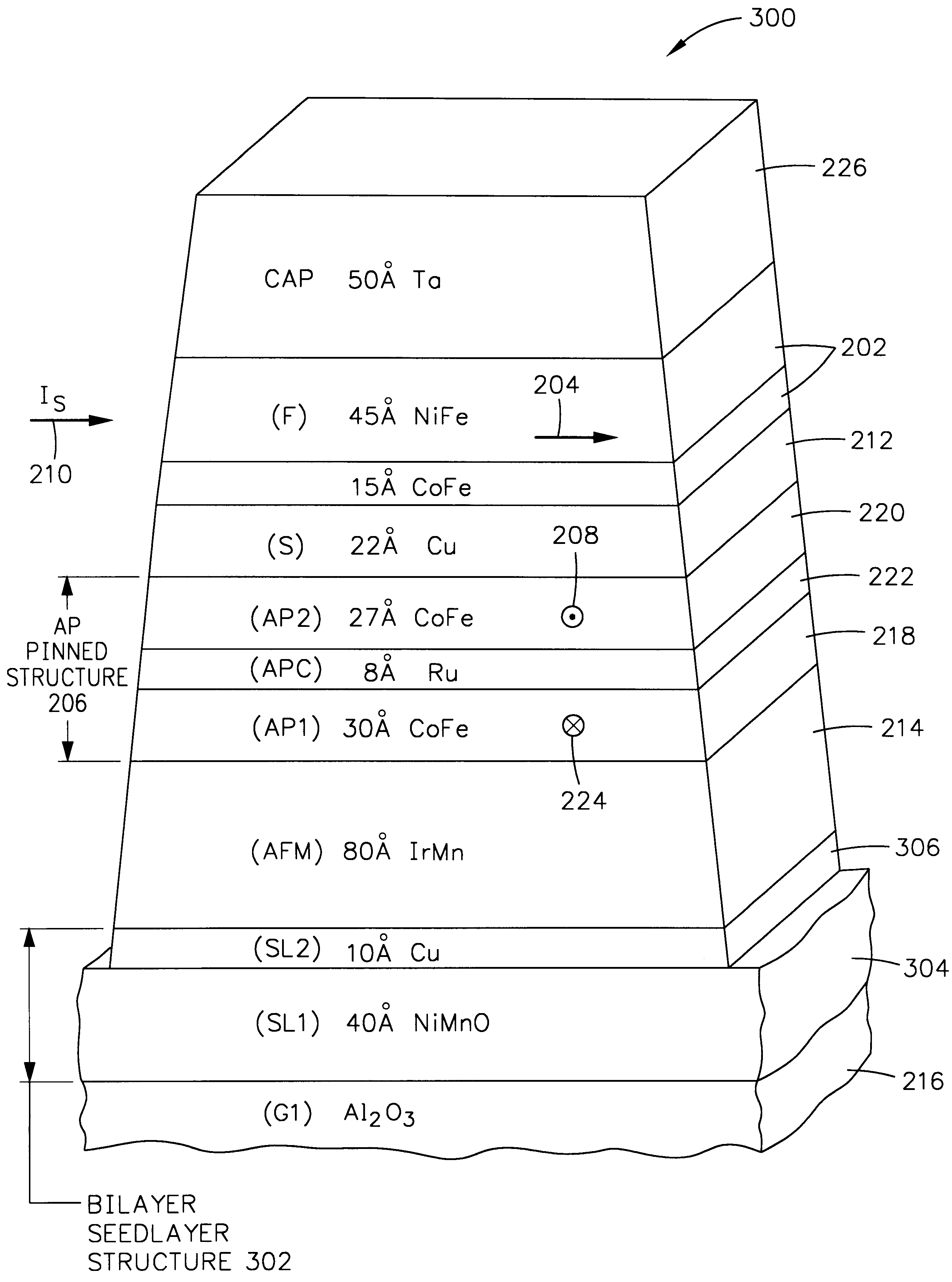
The spin valve sensor 300 in FIG. 13 is a first embodiment of the present invention. The spin valve sensor 300 is the same as the spin valve sensor 200 in FIG. 12 except for a seed layer (SL) structure 302 that is located between the first read gap layer 216 and the pinning layer 214. The seed layer structure 302 has a first seed layer (SL1) 304 comprising a metallic oxide and a second seed layer (SL2) 306 comprising a nonmagnetic metal. The first seed layer 304 is located on and interfaces the first read gap layer 216 and the second seed layer 306 interfaces and is located between the first seed layer 304 and the pinning layer 214. In this example, the first seed layer 304 was 40 .ANG. of nickel manganese oxide (NiMnO) and the second seed layer 306 was 10 .ANG. of copper (Cu).

After resetting the pinning layer 214, as discussed hereinabove, the magnetoresistive coefficient (dr / R) of the spin valve sensor 300 was 8.24% and the ferromagnetic coupling field...

example 3

The spin valve sensor 400 shown in FIG. 14 is the same as the spin valve sensor 200 shown in FIG. 12 except the pinned layer structure is a single ferromagnetic pinned layer 402 which, in this example, was 24 .ANG. of cobalt iron (CoFe). The magnetic moment 404 of the pinned layer 402 is shown perpendicular to and toward the ABS. It is the relative rotation between the magnetic moments 204 and 404 that determines the magnetoresistance (dr) of the read sensor 400. This example has no seed layer between the pinning layer 214 and the first read gap layer 216.

After resetting the pinning layer 214, as discussed hereinabove, the magnetoresistive coefficient (dr / R) was 4.0% and the ferromagnetic coupling field (H.sub.F) was 8 Oe. It is an object of the present invention to improve this magnetoresistive coefficient (dr / R).

example 4

Second Embodiment of Invention

The spin valve sensor 500 in FIG. 15 is a second embodiment of the present invention. This spin valve sensor is the same as the spin valve sensor 400 in FIG. 14 except a seed layer structure 502 is employed between the first read gap layer 216 and the pinning layer 214. The seed layer structure 502 comprised a first seed layer (SL1) 504 of a metallic oxide and the second seed layer (SL2) 506 was a nonmagnetic metal. In this sensor the first seed layer 504 was 40 .ANG. of nickel manganese oxide (NiMnO) and the second seed layer 506 was 10 .ANG. of copper (Cu). The first seed layer 504 interfaced and was located on the first read gap layer 216 and the second seed layer 506 was located between and interfaced each of the first seed layer 504 and the pinning layer 214.

After resetting the spin valve sensor 500, as discussed hereinabove, the magnetoresistive coefficient (dr / R) was 5.6% and the ferromagnetic coupling field (H.sub.F) was 0.1 Oe. The magnetoresis...


PUM


Abstract

A bilayer seed layer structure is employed between a first read gap layer and a spin valve sensor for increasing the magnetoresistive coefficient (dr/R). In a bottom spin valve sensor the bilayer seed layer structure is located between the first read gap layer and a pinning layer and in a top spin valve sensor the bilayer seed layer structure is located between the first read gap layer and the free layer. The pinning layer is preferably iridium manganese (IrMn). The bilayer seed layer structure includes a first seed layer which is a metallic oxide and a second seed layer that is a nonmagnetic metal. A preferred embodiment is a first seed layer of nickel manganese oxide (NiMnO) and a second seed layer of copper (Cu).

Description

1. Field of the InventionThe present invention relates to a seed layer structure for a spin valve sensor and, more particularly, to a bilayer seed layer structure which increases a magnetoresistive coefficient of the spin valve sensor by improving its microstructure.2. Description of the Related ArtThe heart of a computer is an assembly that is referred to as a magnetic disk drive. The magnetic disk drive includes a rotating magnetic disk, a slider that has write and read heads, a suspension arm that supports the slider above the rotating disk and an actuator that swings the suspension arm to place the read and write heads over selected circular tracks on the rotating disk. The suspension arm biases the slider into contact with the surface of the disk when the disk is not rotating but, when the disk rotates, air is swirled by the rotating disk adjacent an air bearing surface (ABS) of the slider causing the slider to ride on an air bearing a slight distance from the surface of the ro...

Claims


Application Information

Patent Timeline
IPC IPC(8): H01F10/32G11B5/39H01F10/00G11B5/31H01F10/08H01F10/12H01F10/30H01L43/08
CPCB82Y10/00B82Y25/00G11B5/3903H01F10/3268G11B5/3967H01F10/3295G11B2005/3996G11B5/39
Inventor PINARBASI, MUSTAFA
Owner HITACHI GLOBAL STORAGE TECH NETHERLANDS BV
Why Eureka
Try Eureka