Product and process for forming a semiconductor structure on a host substrate

a technology of host substrate and semiconductor structure, which is applied in the direction of crystal growth process, polycrystalline material growth, chemically reactive gas, etc., can solve the problems of poor carrier mobility of less than 1 cm.sup.2/vs, high disorder, and large dislocation density of materials

Inactive Publication Date: 2001-04-03
IBM CORP
View PDF2 Cites 103 Cited by
  • Summary
  • Abstract
  • Description
  • Claims
  • Application Information

AI Technical Summary

Benefits of technology

The layer of nitride material is comprised of one or more nitride films selected from the group of gallium nitride, aluminum nitride or indium nitride and / or their alloys. Next, one or more layers of substantially single crystal or polycrystalline semiconductor material are grown on the layer of nitride material. The layer or layers of silicon material form a semiconductor structure. Then, a composite structure is formed of the sapphire substrate, the layer of nitride material, the semiconductor structure and the host substrate. The back surface of the sapphire substrate is laser irradiated with sufficient energy to substantially dissociate enough nitrogen from the nitride material to allow the sapphire substrate to be lifted from the composite structure. The sapphire substrate is then lifted from the composite structure. Any metallic residue is removed from the composite structure.

Problems solved by technology

The problem arises because glass is an amorphous substrate.
In the limiting case of very small grains, there is a consequent high degree of disorder.
36, pages 741 to 743, 1980, a single crystal silicon grown on sapphire substrates, with a high lattice mismatch resulting in a very large density of dislocations.
However, these materials also suffer from poor carrier mobilities of less than 1 cm.sup.2 / Vs.
The problem essentially is how to form single crystal thin silicon films onto large area glass or plastic substrates in an economical fashion to create high mobility devices that provide a better alternative to amorphous silicon on glass or organic electronics on plastic.
Growth of a single crystal film on an amorphous substrate is an unsolved challenge.
There are different ways of transferring a silicon layer to an arbitrary substrate, most of which are uneconomical or impractical.
However, this method destroys an entire silicon wafer such that a large area coating is therefore uneconomical.
However, a smartcut process requires a 600.degree. C. anneal, which is incompatible with commonly used glass or plastic substrates.

Method used


Image

  • Product and process for forming a semiconductor structure on a host substrate
  • Product and process for forming a semiconductor structure on a host substrate

Examples


Embodiment Construction

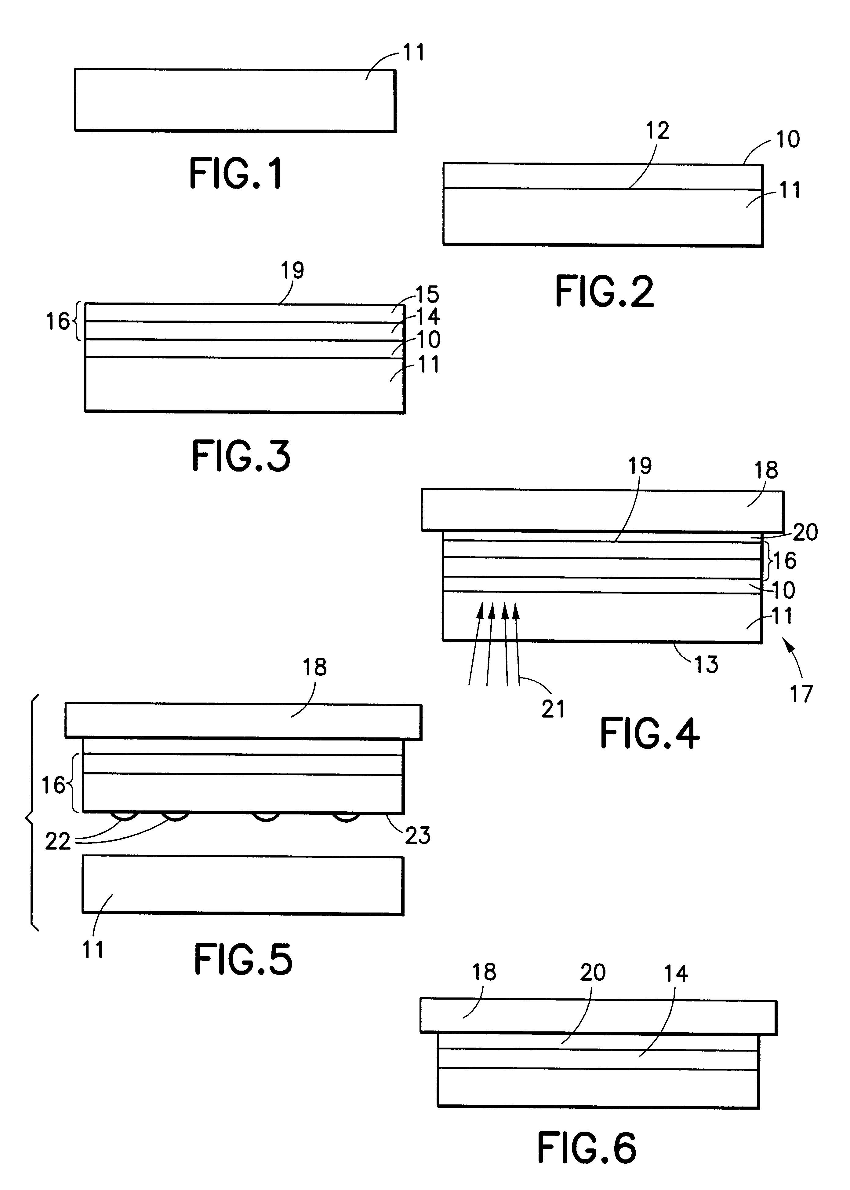
The process, according to the present invention, forms a substantially single crystal or polycrystalline semiconductor layer on a host substrate, at relatively low temperature. The process is non-destructive in the sense that a single sapphire substrate can be re-used consistently to transplant the semiconductor onto the host substrate.

The process is applicable to column IV semiconductors, and is especially applicable to silicon and germanium as they have the same diamond cubic crystal structure and lattice constants that are within about 4% of one another. For ease of description, the semiconductor will be referred to herein as silicon, it being understood that other column IV semiconductors can be used, especially germanium.

The host substrate can be any substrate. Preferably, the host substrate is glass, metal. a polymeric material or a semiconductive material.

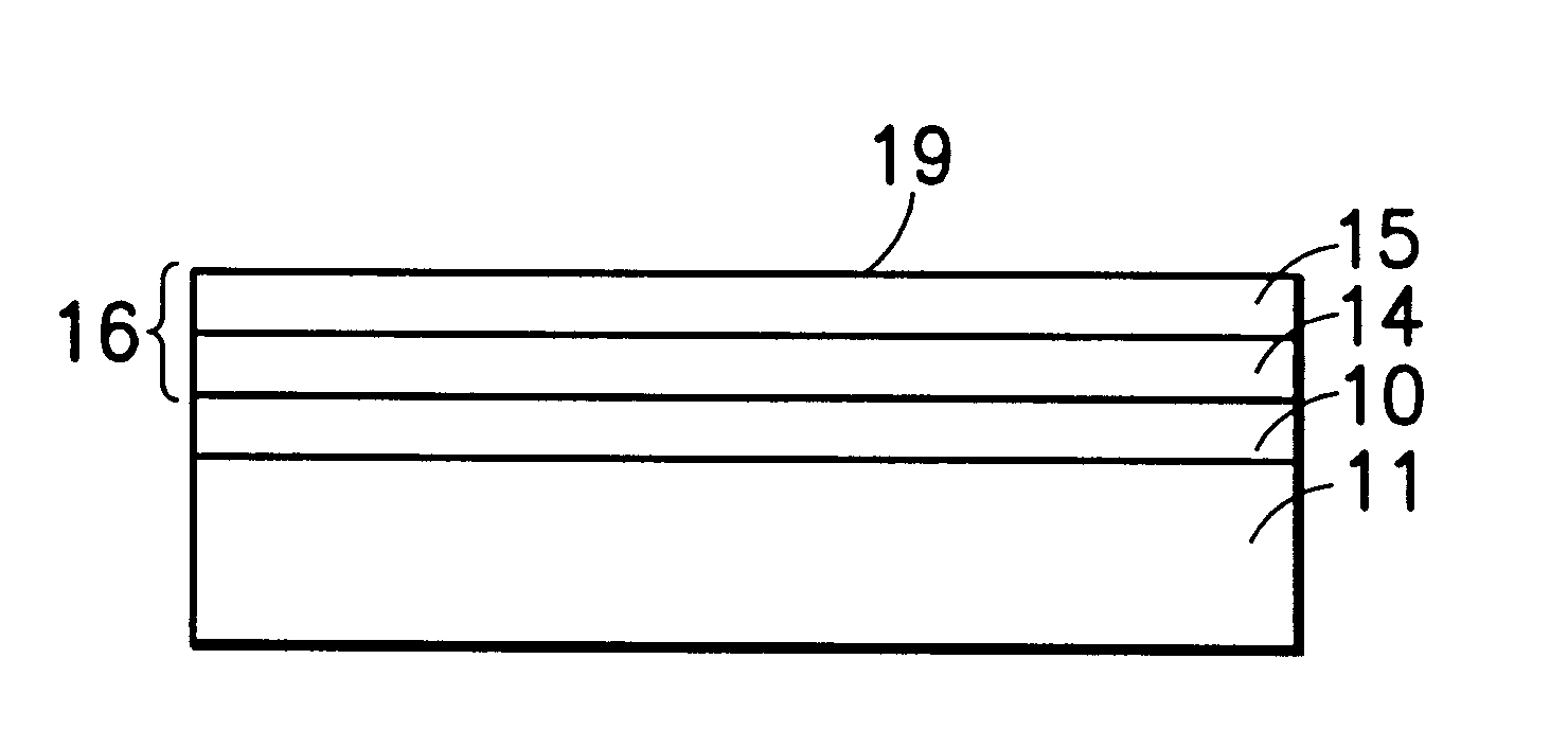
With reference to FIGS. 1 through 6, a thin layer of wide band gap nitride material 10 is deposited or grown on a top surf...


PUM

PropertyMeasurementUnit
depthaaaaaaaaaa
depthaaaaaaaaaa
energy absorption depthaaaaaaaaaa

Abstract

A process for cheaply fabricating a substantially single crystal or a polycrystalline semiconductor structure on a host substrate. The process begins by depositing a layer of wide band gap nitride material 10, such as gallium nitride, aluminum nitride and/or indium nitride, on a sapphire substrate 11. The semiconductor structure 14 is then grown on the nitride layer. Next, the host substrate 15 is attached with a bonding agent to an exposed surface area of the semiconductor structure 14. The sapphire substrate is lifted off by irradiation in which nitrogen is dissociated from the nitride layer.

Description

This invention relates to semiconductor fabricating processes and to products made by such processes. In particular, the invention relates to a process for forming a substantially single crystal semiconductor structure on a host substrate, such as glass, polymeric materials, semiconductive materials, or metal.BACKGROUND OF INVENTIONSilicon based microelectronic drive circuits deposited on glass substrates are used extensively in the liquid crystal display. Presently, the silicon used is amorphous or near amorphous in structure. Consequently, the silicon exhibits carrier mobilities that are less than one centimeter squared per volt-second (1 cm.sup.2 / Vs). The problem arises because glass is an amorphous substrate. Hence, any silicon deposited on glass is either amorphous or polycrystalline. Instead, it is desirable to prepare a single crystal film of silicon on a glass substrate in an economical manner, since single crystal films have much higher carrier mobilities.Polycrystalline s...

Claims


Application Information

Patent Timeline
Patent Type & Authority Patents(United States)
IPC IPC(8): H01L21/02H01L21/20H01L21/70H01L21/762H01L33/00H01L21/205
CPCH01L21/2007H01L21/76251H01L33/007H01L33/0079Y10S148/093Y10S148/094H01L33/0093H01L21/02389
Inventor BOJARCZUK, NESTOR A.GUHA, SUPRATIKGUPTA, ARUNAVA
Owner IBM CORP
Why Eureka
Try Eureka