
Kernel-based fast aerial image computation for a large scale design of integrated circuit patterns

a large-scale design and image computation technology, applied in the field of aerial images for photolithographic simulation, can solve the problems of inability to compute images of large masks in a reasonable amount of time, large size of data representing typical ic patterns, and high computational intensity of all

Inactive Publication Date: 2001-04-24
IBM CORP
View PDF2 Cites 130 Cited by
  • Summary
  • Abstract
  • Description
  • Claims
  • Application Information

AI Technical Summary

Benefits of technology

Accordingly, an object of the present invention is to provide aerial images for photolithographic simulation which can be advantageously produced during the exposure step of a photo-lithographic process in the design of a semiconductor integrated circuit wafer.
It is another object of the invention to provide an efficient computation of aerial images for large mask areas and for arbitrary photomask patterns.

Problems solved by technology

One of the main challenges to using model-based simulators in integrated circuit (IC) mask applications is the formidable size of the data representing a typical IC pattern.
Since all steppers employ partially coherent illumination, such modeling is computationally intensive for all but elementary patterns.
Although SPLAT has been extensively used in conventional lithography simulation, it is incapable of computing images of large masks in a reasonable amount of time.
However, as these are commercial products, no details are available as to the particular methods used to compute the images.
The main drawback of SPLAT in IC lithography applications is the large computation time required for large mask areas because its computation time increases as the fourth power of the linear dimension.
The aforementioned prior art approach uses finitely supported rectangles, wherein each resizing of the rectangle must be handled individually, a distinct disadvantage.

Method used


Image

  • Kernel-based fast aerial image computation for a large scale design of integrated circuit patterns
  • Kernel-based fast aerial image computation for a large scale design of integrated circuit patterns
  • Kernel-based fast aerial image computation for a large scale design of integrated circuit patterns

Examples


Embodiment Construction

Theory of Aerial Image Formation

Aerial image formation can be described by the following basic equation 1: ##EQU1##

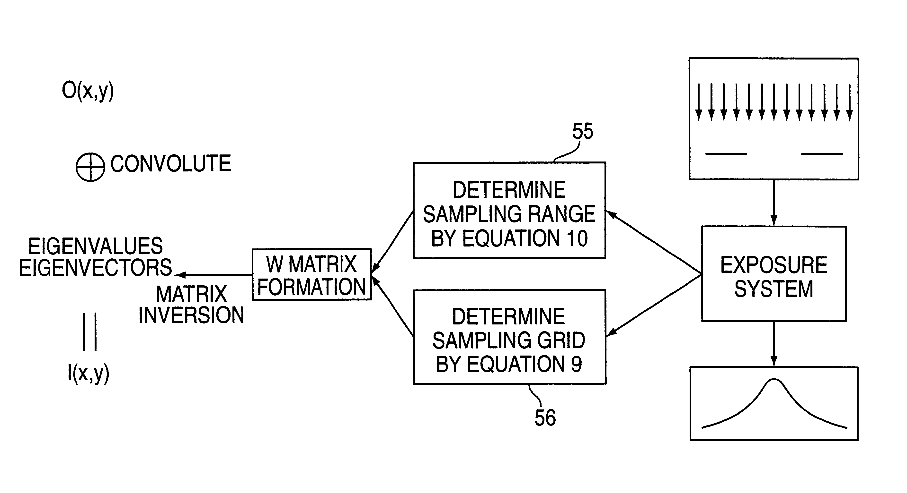
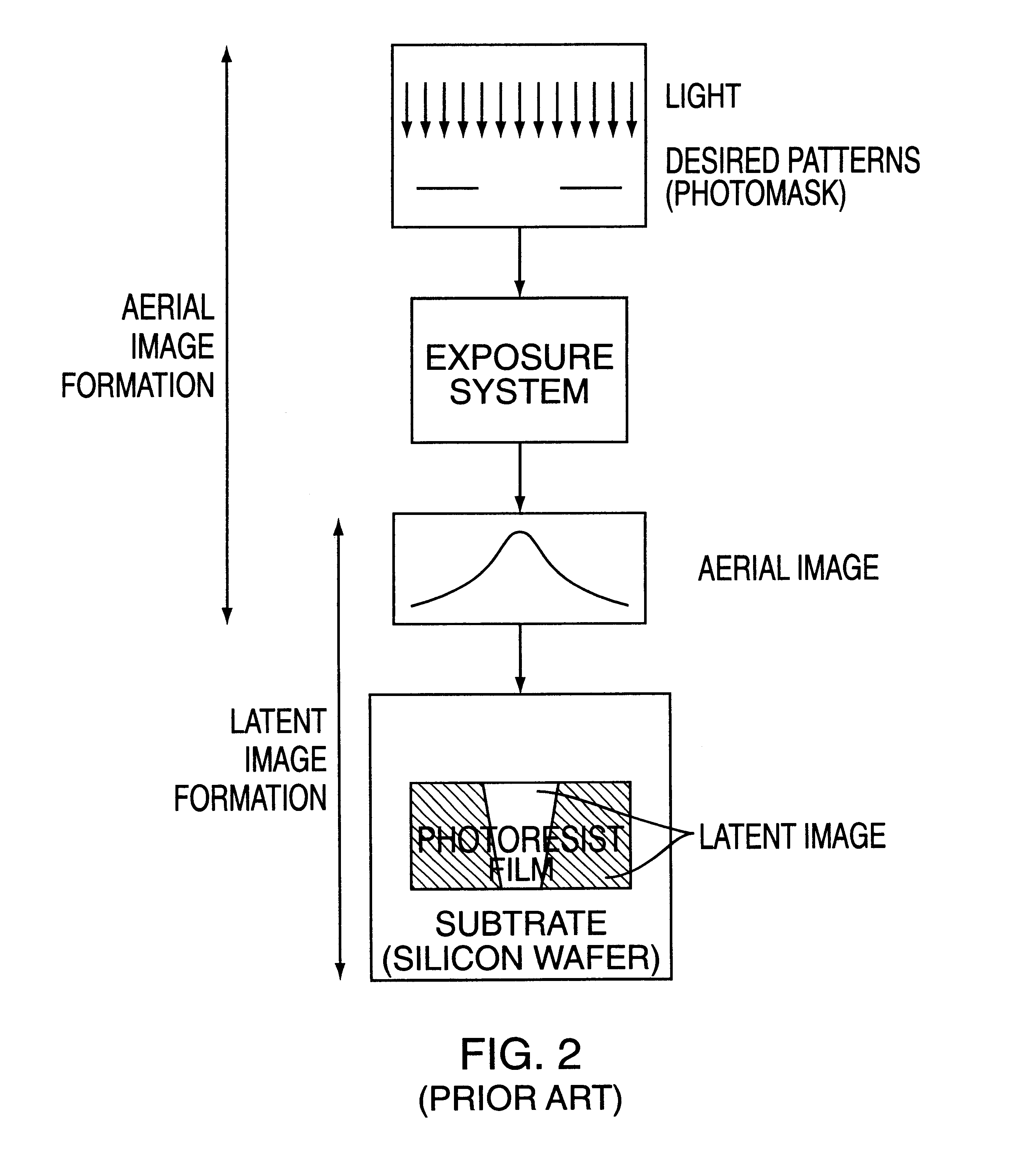
with i=-1, denoting complex conjugation, (x', y') and (.alpha.', .beta.', .gamma.') representing, respectively, the image plane coordinates and directional cosines of the exit pupil, assuming that the optic axis is aligned with the z-axis and light propagates in the +z direction. Essentially, J(x,y) represents the light source of the exposure system, Po.sub.(x,y) describes the imaging of the exposure system, and Po.sub.(x,y) the function of the photomask patterns.

Aerial Image Calculation via Transmission Cross-coefficients (TCC)

For computation sake, equation 1 can be expressed by substituting equation 3 into equation 1. After some Mathematical manipulation, the following equation 4 results: ##EQU2##

are called the transmission cross-coefficients (TCCs).

are referred to as transmission cross-coefficients (see Principles of Oitics, section 10.5, pp. 528-532, by M. Born et a...


PUM


Abstract

A method of simulating aerial images of large mask areas obtained during the exposure step of a photo-lithographic process when fabricating a semiconductor integrated circuit silicon wafer is described. The method includes the steps of defining mask patterns to be projected by the exposure system to create images of the mask patterns; determining an appropriate sampling range and sampling interval; generating a characteristic matrix describing the exposure system; inverting the matrix to obtain eigenvalues as well as the eigenvectors (or kernels) representing the decomposition of the exposure system; convolving the mask patterns with these eigenvectors; and weighing the resulting convolution by the eigenvalues to form the aerial images. The method is characterized in that the characteristic matrix is precisely defined by the sampling range and the sampling interval, such that the sampling range is the shortest possible and the sampling interval, the largest possible, without sacrificing accuracy. The method of generating aerial images of patterns having large mask areas provides a speed improvement of several orders of magnitude over conventional approaches.

Description

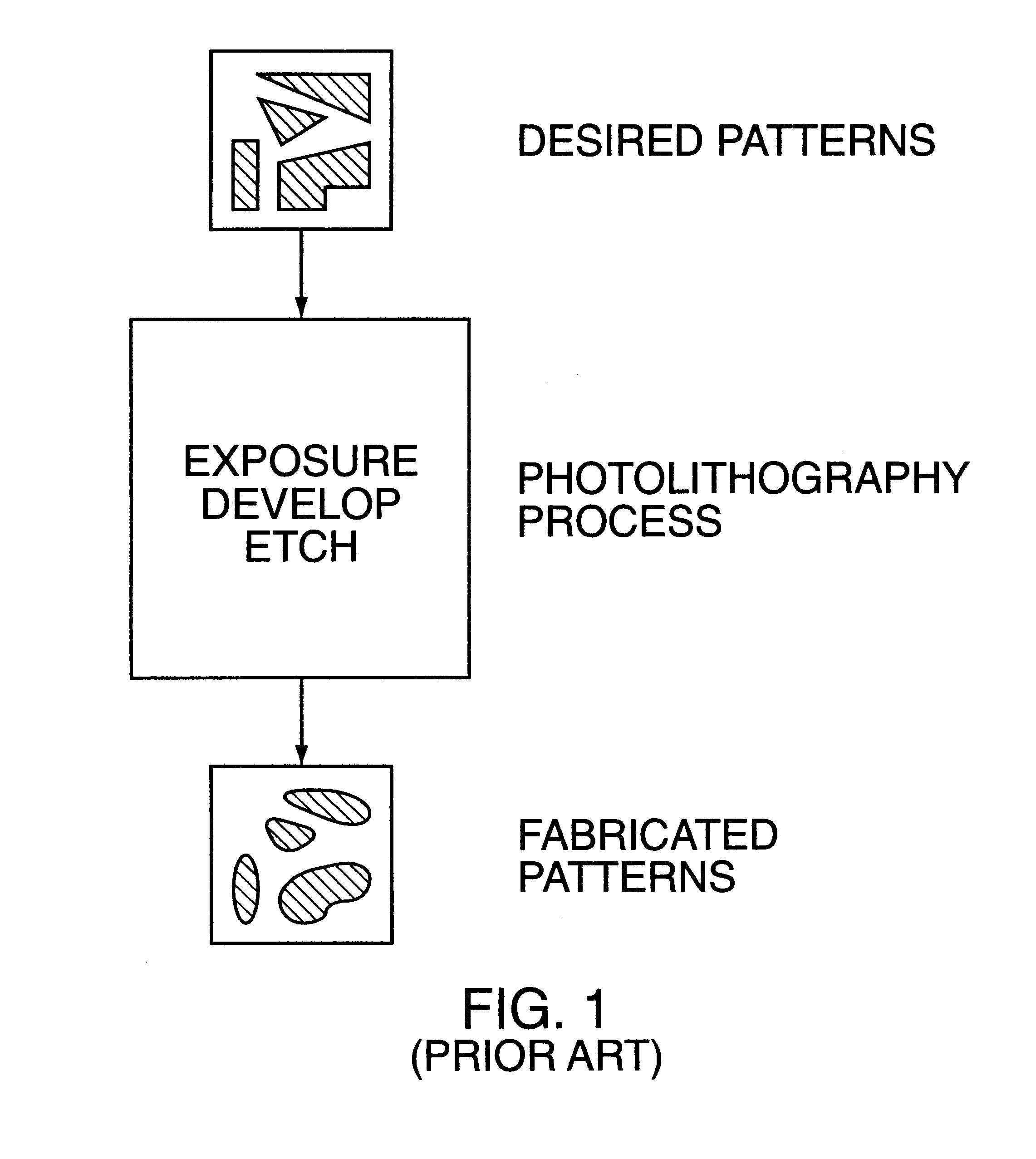
This invention relates generally to the field of photo-lithography, and more particularly, to the simulation of aerial images during the exposure step of a photo-lithographic process and specifically tailored for the design and fabrication of large scale semiconductor integrated circuits.The photo-lithography process in semiconductor fabrication consists in duplicating desired circuit patterns as best as possible onto a semiconductor wafer. This process, shown in FIG. 1, is conventionally subdivided into three steps: exposure, develop, and etch. The exposure step projects the desired circuit patterns onto a film of photosensitive material commonly referred to as photoresist. The desired circuit patterns are typically represented as opaque (or translucent in some cases) and transparent regions on a template commonly called a photomask. Semiconductor circuits are then repeatedly reproduced from this template by a variety of techniques, among them projection being the most popular for ...

Claims


Application Information

Patent Timeline
IPC IPC(8): G03F7/20
CPCG03F7/705
Inventor WONG, ALFRED K.FERGUSON, RICHARD A.
Owner IBM CORP
Learn More