Method for fabricating semiconductor integrated circuit device

a technology of integrated circuit devices and semiconductors, applied in the direction of semiconductor devices, basic electric elements, electrical apparatus, etc., can solve the problems of difficult known oxidation formation methods, unsatisfactory formation of thicker films, and liable production of structural defects such as si-h bonds, si-oh bonds and the lik

Inactive Publication Date: 2001-05-29
RENESAS ELECTRONICS CORP
View PDF20 Cites 34 Cited by
  • Summary
  • Abstract
  • Description
  • Claims
  • Application Information

AI Technical Summary

Problems solved by technology

However, it is indicated that the above combustion system has the problem: since hydrogen is ignited and burnt while being injected from a quartz nozzle attached at the tip of a hydrogen gas supply pipe, the resultant flame comes too near to the nozzle under conditions where the amount of hydrogen is too small; and the nozzle eventually melts by application of heat thereto to cause particles to be generated, which serve as a pollution source of a semiconductor wafer (on the contrary, if the amount of hydrogen is increased in excess, the resultant flame arrives at an end portion of the combustion tube, so that the quartz walls are caused to be melted, thereby generating particles, or the flame is cooled at the wall surfaces and may be put out, thereby presenting a problem on safety).
As a result, structural defects such as of an Si--H bond, an Si--OH bond and the like are liable to be produced in the thin film or at the interface with a silicon substrate.
According to the studies made by us, known oxidation formation methods are difficult in forming a very thin gate oxide film of a high quality and with a thickness of 5 nm or below (although it is as a matter of fact that similar effects can be expected when the thickness is 5 nm or over) in a uniform thickness and in high fidelity.
Needless to say, the formation of a thicker film is also unsatisfactory in many respects.
However, a thin natural oxide film is inevitably formed on the wafer surface on the way of transferring the wafer from the wet cleaning step to an oxidation step.
Moreover, in the oxidation step, an undesirable initial oxide film is formed on the wafer surface by contact with oxygen in the oxidation species prior to intended oxidation.
Nevertheless, when a very thin oxide film is formed according to known oxide film formation methods, the ratio of these lower-quality films rather increases.
More particularly, if a very thin film is formed according to the known oxide film formation method, not only uniformity and fidelity of a film thickness are not assured, but also the quality of the film lowers.
Therefore, it will be apparent that these methods cannot be applied to a mass-production process of semiconductor integrated circuits as they are.

Method used


Image

  • Method for fabricating semiconductor integrated circuit device
  • Method for fabricating semiconductor integrated circuit device
  • Method for fabricating semiconductor integrated circuit device

Examples


Embodiment Construction

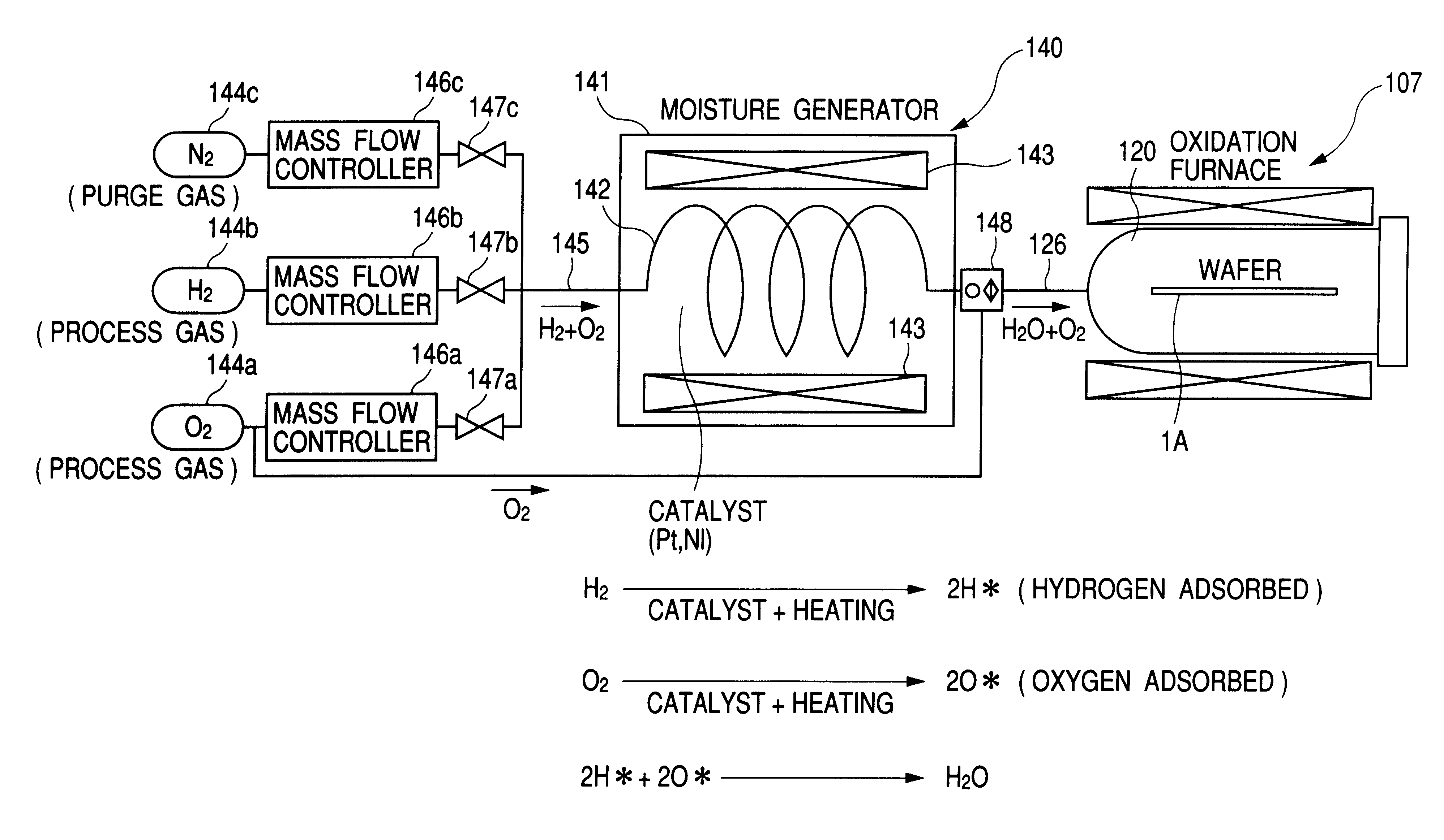
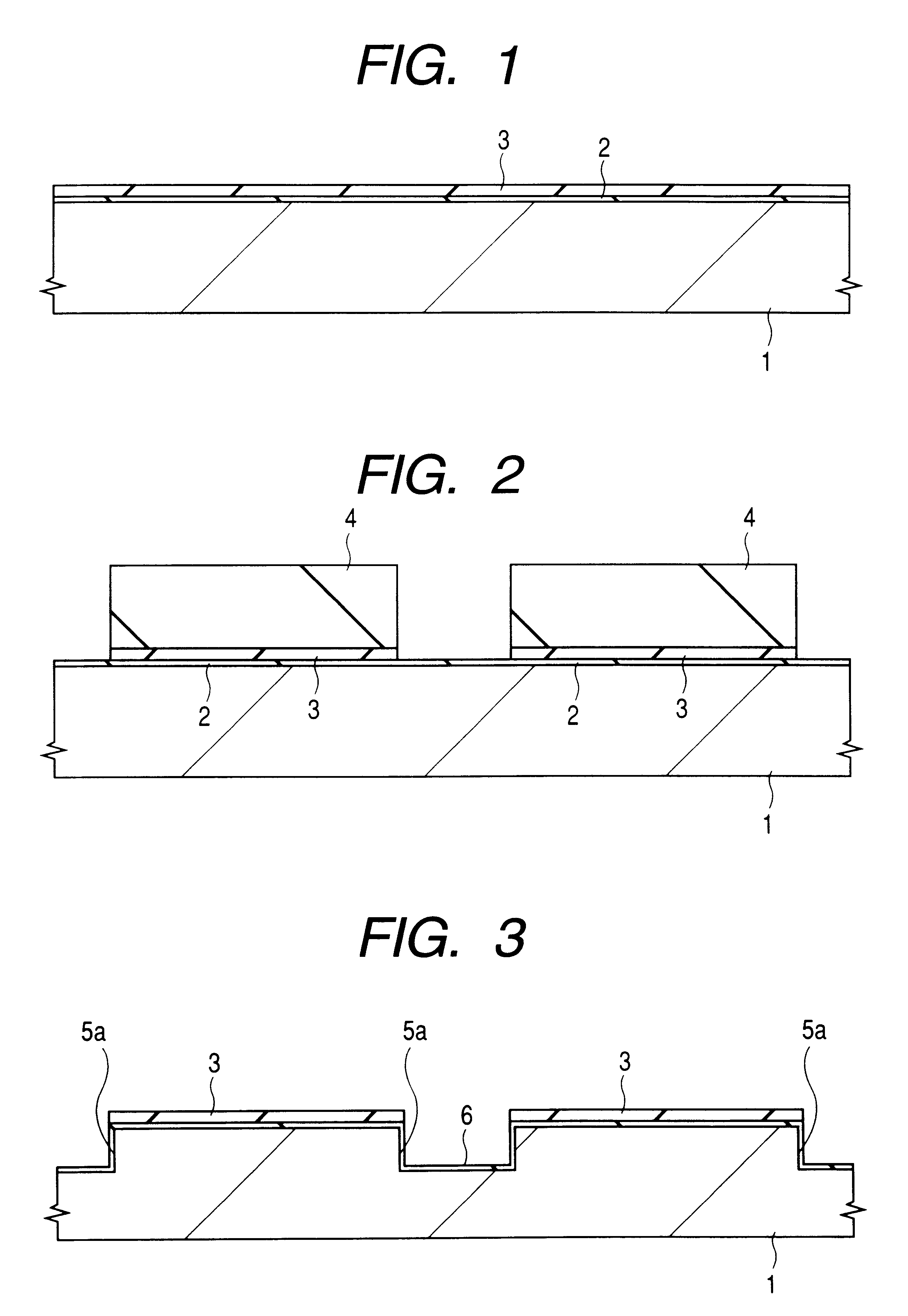
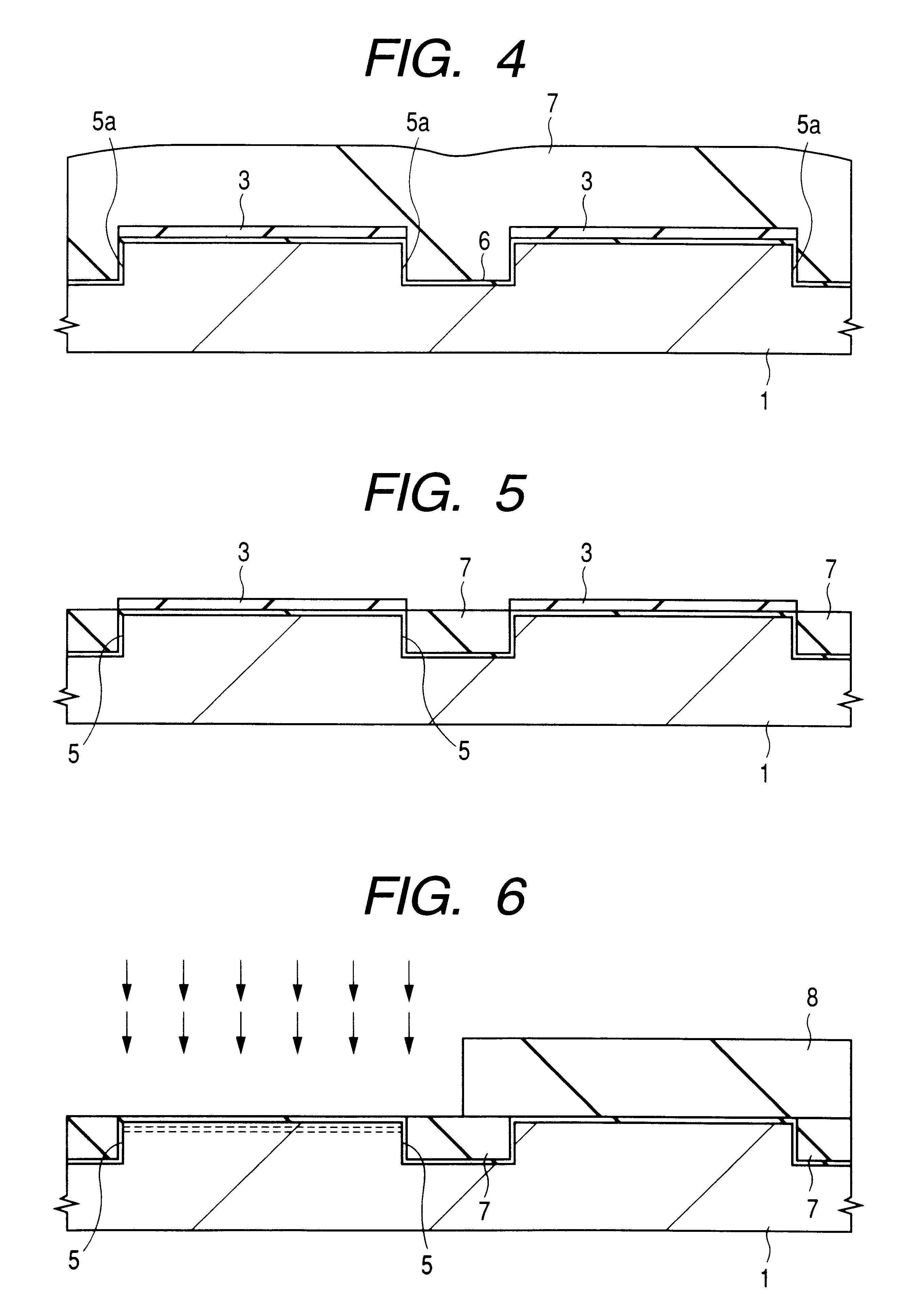
The embodiments of the invention are described in details based on the accompanying drawings. Throughout the drawings for illustrating the embodiments of the invention, like reference numerals indicate like members having a like function and are not repeatedly illustrated.

For convenience's sake, the invention is described by division into several examples or items, but it is a matter of fact that these embodiments or items are not independent, but have interrelations with each other to constitute modifications of other embodiments, details of a specific step or process, or devices used in some steps. More particularly, if individual apparatus or unit processes illustrated in one embodiment may be applicable to other embodiments as they are, these apparatus or unit processes are not repeatedly described in other embodiments. On the contrary, where individual apparatus or unit processes, which are independently illustrated, may be applied to other embodiments as they are, these are no...


PUM

PropertyMeasurementUnit
temperatureaaaaaaaaaa
lengthaaaaaaaaaa
lengthaaaaaaaaaa

Abstract

A method for fabricating a semiconductor integrated circuit device of the invention comprises feeding oxidation species containing a low concentration of water, which is generated from hydrogen and oxygen by the catalytic action, to the main surface of or in the vicinity of a semiconductor wafer, and forming a thin oxide film serving as a gate insulating film of an MOS transistor and having a thickness of 5 nm or below on the main surface of the semiconductor wafer at an oxide film-growing rate sufficient to ensure fidelity in formation of an oxide film and uniformity in thickness of the oxide film.

Description

TECHNICAL FIELDThis invention relates to a method for fabricating semiconductor integrated circuit devices including semiconductor devices, and more particularly, to a technique useful for application to the formation of gate oxide films (insulating films) such as of MOSFET (metal oxide semiconductor field effect transistor).BACKGROUND ARTIn the initial stage of semiconductor industries, bubbling was in wide use where a carrier gas such as oxygen or the like was passed through water in a bubbler. Although this technique was advantageous in that a wide range of a moisture content could be covered, a problem on pollution could not be avoided, and thus, the technique is rarely used at present. Accordingly, an oxygen and hydrogen combustion method, i.e. a pyrogenic system, has been widespread in order to avoid the disadvantage of the bubbler.Disclosure of Prior Art Literature, etc.With regard to an improvement in thermal oxidation and a moisture generation method therefor, to which the ...

Claims


Application Information

Patent Timeline
Patent Type & Authority Patents(United States)
IPC IPC(8): H01L21/70H01L21/28H01L21/02H01L29/423H01L21/314H01L21/316H01L21/8238H01L29/40H01L21/00H01L21/306H01L21/31H01L21/336H01L21/469H01L21/76H01L29/51
CPCH01L21/02255H01L21/28185H01L21/28194H01L21/28202H01L21/28211H01L21/3144H01L21/31658H01L21/31662H01L21/67109H01L21/67167H01L21/67173H01L21/67213H01L21/67219H01L21/823807H01L21/823814H01L21/823857H01L29/42364H01L29/518H01L21/02238H01L21/02052Y10S148/023Y10S438/935Y10S148/116H01L21/18
Inventor TANABE, YOSHIKAZUSAKAI, SATOSHINATSUAKI, NOBUYOSHI
Owner RENESAS ELECTRONICS CORP
Why Eureka
Try Eureka