Semiconductor display device

a display device and semiconductor technology, applied in the direction of static indicating devices, identification means, instruments, etc., can solve the problems of not having a preferred effect, taking a long time to perform the process, and still leaving a problem in respect of productivity (throughput)

Inactive Publication Date: 2001-06-12
SEMICON ENERGY LAB CO LTD
View PDF6 Cites 65 Cited by
  • Summary
  • Abstract
  • Description
  • Claims
  • Application Information

AI Technical Summary

Problems solved by technology

However, there is almost no preferred effect at a temperatures of 500.degree. C. or below.
The first method involves a problem of taking a long time to perform the process.
Thus a problem has still been left in respect of productivity (throughput).
However, where applying the above technique using linear pulse laser irradiation with overlap while slight shifting, linear fringes naturally occur on a surface of a laser-irradiated semiconductor material.
These fringes has a great adverse effect upon characteristics of a device having been formed or to be formed on the surface of the semiconductor material.
In particular, a serious problem will be encountered when a plurality of devices are to be formed on the substrate with an even characteristic on a one-by-one device basis.
In also the anneal method using a linear laser light, a problem rises in respect of evenness by the effect of irradiation.
However, in the case that a multiplicity (on the order of several millions to several tens of millions) of thin film transistors are required to form on a glass substrate as in an ac

Method used


Image

  • Semiconductor display device
  • Semiconductor display device
  • Semiconductor display device

Examples


embodiment 2

The active matrix liquid crystal display device of the present invention stated in Embodiment 1 is fully cope with as an active matrix liquid crystal display device with high precision and resolution. The number of pixels is great enough to cope with a future ATV (Advanced TV). It is therefore possible to cope with an active matrix liquid crystal display device with a resolution higher than XGA, e.g., 1920 in horizontal.times.1280 in vertical.

embodiment 3

The active matrix liquid crystal display devices as stated in the above embodiments 1 and 2 are applicable as a transparent type active matrix liquid crystal display and as a reflective type active matrix liquid crystal display device. Meanwhile, the liquid crystal material can use an antiferroelectric liquid crystal having no threshold. Also, the liquid crystal material can use a ferroelectric liquid crystal. This can cope with a case where the memory effect of the ferroelectric liquid crystal is erased by an especial orientation film or the like.

Explanations were made in the above embodiments 1 and 2 for the case that the liquid crystal is used as a display medium. However, these structures may be applied for any other semiconductor display device having a display medium having an optical characteristic to be modulated responsive to voltage application. For example, an electroluminescence element or electrochromics element may be used as a display medium.

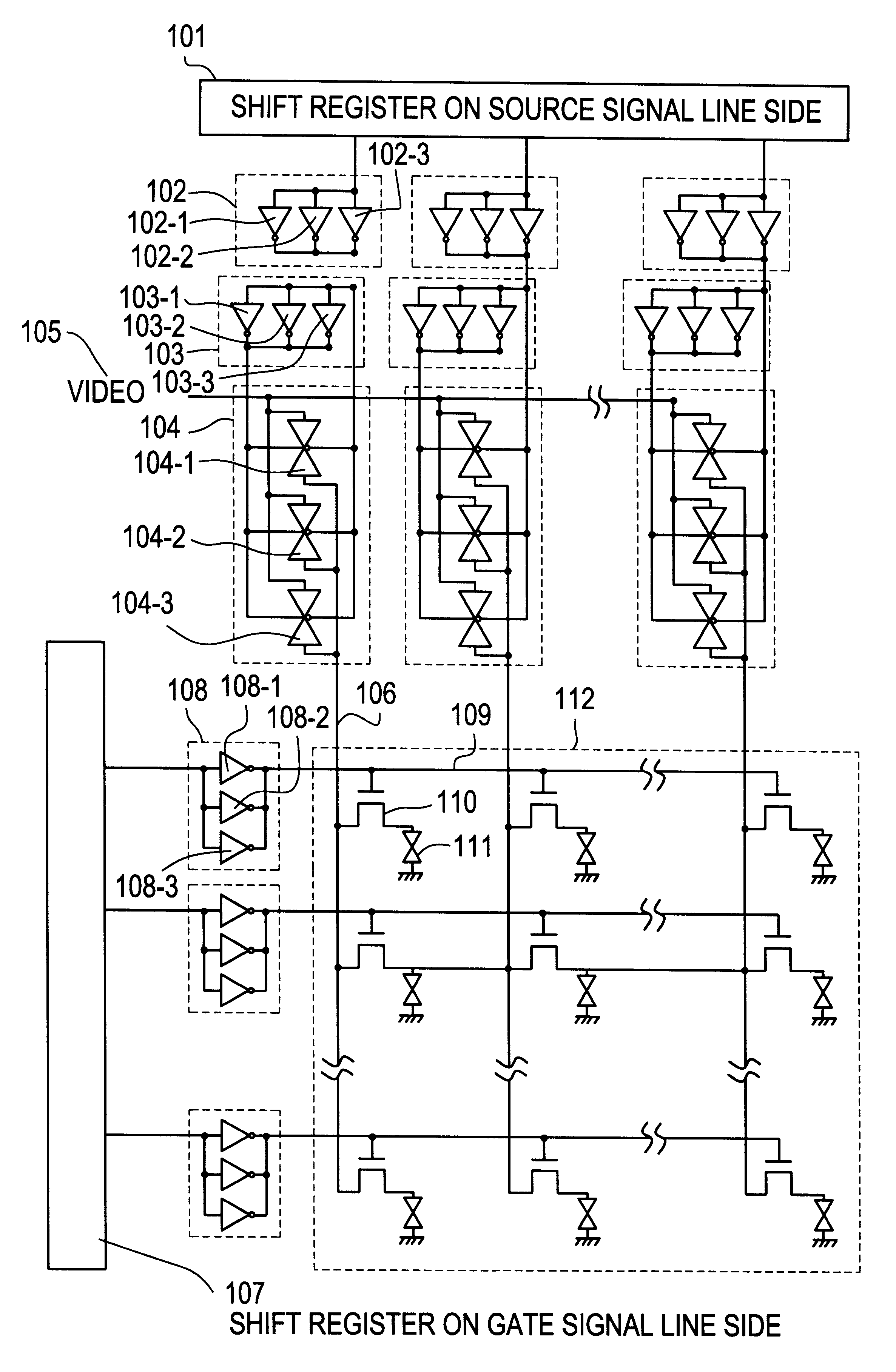
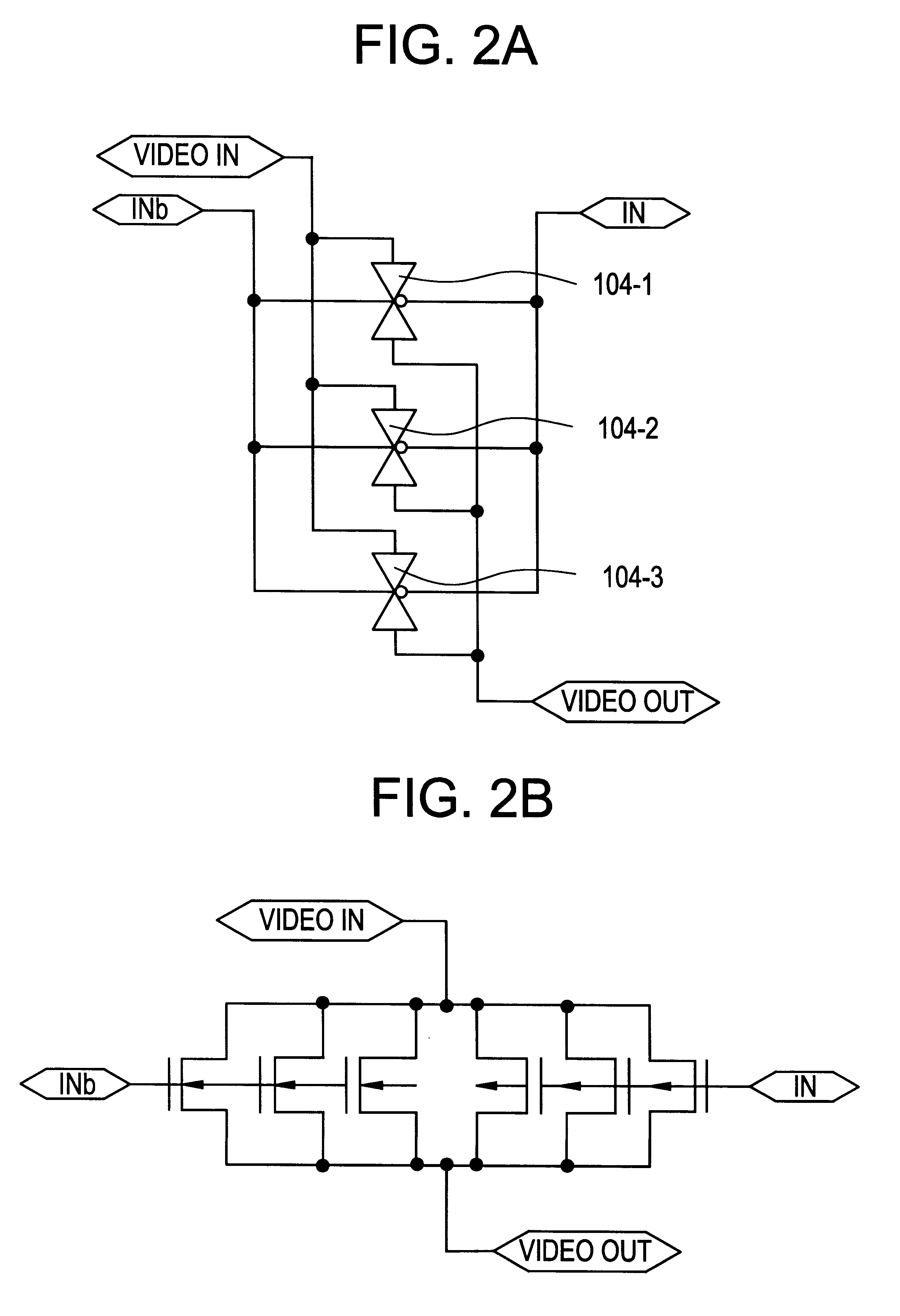
The TFTs employed for the ...

embodiment 4

The semiconductor display devices of Embodiments 1-3 described above have a variety of applications. In this embodiment a semiconductor device built with an active matrix semiconductor display device of the present invention.

Such semiconductor devices include video cameras, still cameras, projectors, head-mount displays, automobile navigators, personal computers, portable information terminals (mobile computers, handy phones, etc.) and so on. Examples of them are demonstrated in FIG. 7.

FIG. 7(A) is a handy phone, which is structured by a main body 701, a sound an output section 702, a sound input section 703, a semiconductor display device 704, an operation switch 705 and an antenna 706.

FIG. 7(B) is a video camera structured by a main body 707, a semiconductor display device 708, a sound input section 709, an operation switch 710, a battery 711 and a picture receiving section 712.

FIG. 7(C) is a mobile computer structured by a main body 713, a camera section 714, a picture receiving ...


PUM


Abstract

An active matrix semiconductor device is provided which is free of unevenness in image. The analog switch and buffer in a drive circuit are structured by a plurality of parallel-connected analog switches and buffers each formed by a TFT with a small channel width. The carrier moving direction of these TFTs are oblique relative to a scanning direction of a linear laser used for laser crystallization. By doing so, the analog switch and the buffer are decreased in characteristic variation with deterioration suppressed. Thus an active matrix semiconductor device is realized which is free of unevenness in image.

Description

1. Field of the InventionThe present invention relates to semiconductor display devices with thin film transistors. More particularly, the invention relates to a technology to manufacture a plurality of thin film transistors free of characteristic variations through the use of a linear laser beam.2. Description of the Prior ArtIn recent years studies have been eagerly made in order to decrease the process temperature in the manufacture of thin film transistors (hereinafter referred to as TFTs). The major reason for this is due to a necessity that a semiconductor device is to be formed on an insulator substrate of such as a glass that is low in cost but high in processability. The temperature decrease in the process to manufacture a semiconductor device is also demanded from a viewpoint of put forward with device scale down and multilevel structure.The manufacture of a high performance semiconductor device requires a process to crystallize an amorphous ingredient or amorphous semicon...

Claims


Application Information

Patent Timeline
IPC IPC(8): G09G3/36H01L27/115G02F1/1362G02F1/13H04M1/02G02F1/136G02F1/133G02F1/1368G09F9/33H01L21/336H01L29/786
CPCG09G3/3677G09G3/3688H01L27/115G02F1/13454G09G2300/0408G09G2320/02H10B69/00
Inventor YAMAZAKI, SHUNPEI
Owner SEMICON ENERGY LAB CO LTD
Why Eureka
Try Eureka