Top surface imaging technique using a topcoat delivery system

a topcoat and imaging technology, applied in the field of topcoat delivery system, can solve the problems of reduced resolution of projected images, special focus problems of dof lenses, and difficult ic fabrication

Inactive Publication Date: 2001-07-10
BELL SEMICON LLC
View PDF6 Cites 35 Cited by
  • Summary
  • Abstract
  • Description
  • Claims
  • Application Information

AI Technical Summary

Benefits of technology

The forming the underlayer step of the present inventive method may include the step of applying the underlayer with a casting solvent which is an organic based solvent, while the depositing a topcoat layer step includes the step of applying the topcoat layer with a water-based casting solvent. In still another aspect of the present invention, before the silylating step, the inventive method may include the step of stripping the topcoat layer to expose the surface of the underlayer thereby allowing silylation of the imaged surface.

Problems solved by technology

Commensurate with this size reduction, various process limitations have made IC fabrication more difficult.
One problem inherent with photolithography is the Depth Of Focus (DOF) in which the wafer topographic variation of the substrate surface may cause the projected image to exhibit some decreased resolution and other optical distortions.
This focus problem of the DOF lens is especially pronounced in IC designs at the high and low plateaus of the submicron features near the wavelength of light used in the photolithography (i.e., 0.25 .mu.m and smaller).
While this imaging technique satisfactorily addresses many DOF issues, several other problems are inherent with this process.
For example, this conventional silylation technique is relatively time consuming to perform.
Thus, cycle time is increased which in turn reduces efficiency and increases manufacture cost.
Another problem associated with this technique is that during the silylation process, SiO.sub.2 is added to the exposed region.
Accordingly, swelling of the silylated region may occur which often distorts the final resist pattern.
In turn, the feature size of the implant or etch can ultimately be affected.
Accounting for or compensating for such swelling is also difficult to implement since it varies from wafer to wafer.
Therefore, this adverse side effect is not easily reproducible and is most unpredictable.
The primary problem associated with this technique, however, is that the ability to restrict and contain the acid migration of the lithographic pattern is reduced.
Although the penetration depth of the radiation is confined to the top surface, the photoacid generators present in the resist may cause excessive photoacid generation which in turn produce adverse acid migration when overexposed.
For example, too deep a vertical migration of the photo acid also results in adverse lateral erosion of the pattern and the undesirable deposition of residue in the etch.
During the silylation process, hence, the necessary degree of silylation is difficult to control since the depth of the silylating reagent cannot be determined.
In contrast, too shallow a radiation penetration produces inadequate etch selectivity.

Method used


Image

  • Top surface imaging technique using a topcoat delivery system
  • Top surface imaging technique using a topcoat delivery system
  • Top surface imaging technique using a topcoat delivery system

Examples


Embodiment Construction

While the present invention will be described with reference to a few specific embodiments, the description is illustrative of the invention and is not to be construed as limiting the invention. Various modifications to the present invention can be made to the preferred embodiments by those skilled in the art without departing from the true spirit and scope of the invention as defined by the appended claims. It will be noted here that for a better understanding, like components are designated by like reference numerals throughout the various figures.

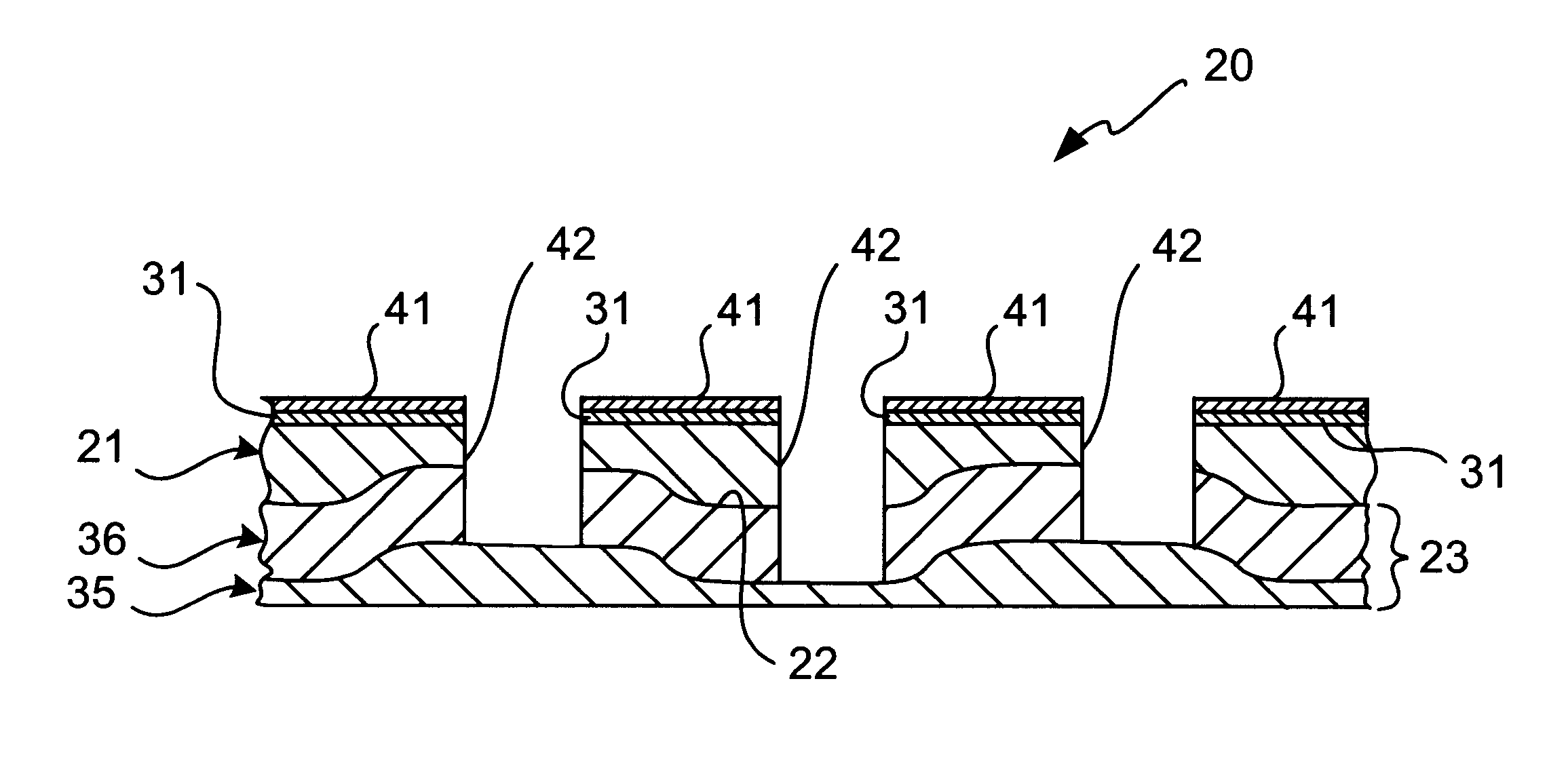
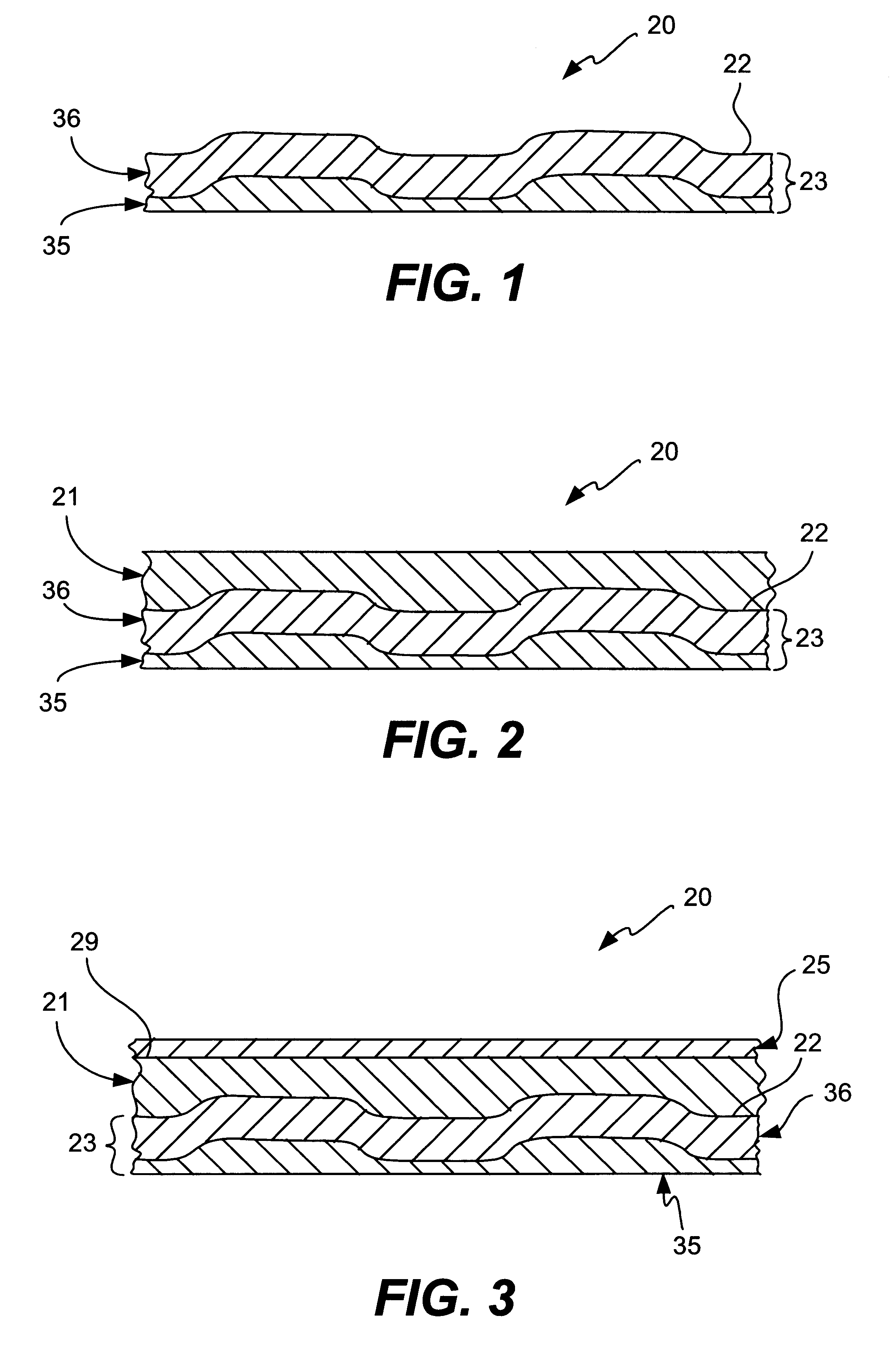
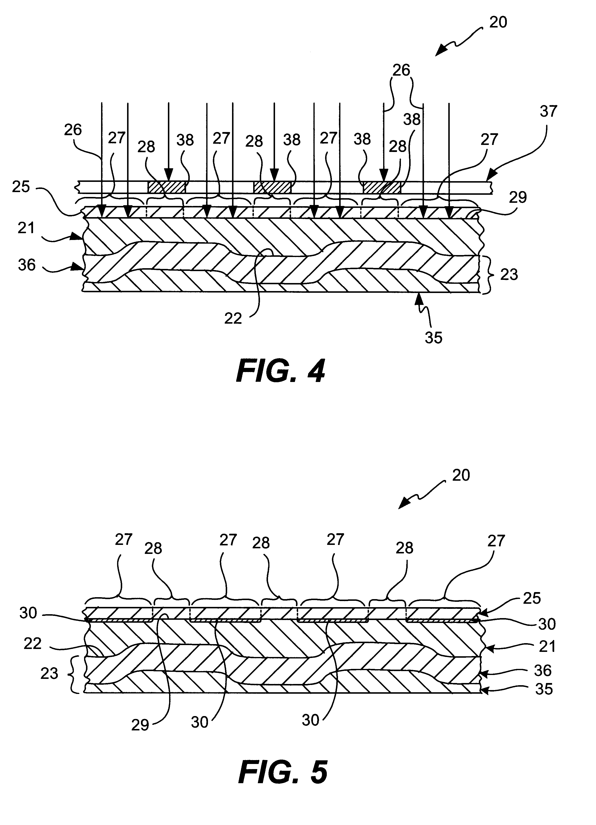
Attention is now directed to FIGS. 1-9 where a method for manufacturing a device, generally designated 20, is provided including the steps of: depositing an underlayer 21 on a first surface 22 of a substrate assembly 23 comprising a first resist material being substantially photoacid generator-free and including an acid liable polymer group (FIG. 2); and depositing a topcoat layer 25 on the deposited underlayer 21 comprising a second res...


PUM

PropertyMeasurementUnit
wavelengthaaaaaaaaaa
temperaturesaaaaaaaaaa

Abstract

An apparatus and method for manufacturing a device using lithography. An underlayer is deposited on a first surface, the underlayer of which is composed of a first resist material adapted to be substantially free of photoacid generators and which includes an acid labile polymer group. A topcoat layer is deposited on top of the underlayer which is composed of a second resist material adapted to be substantially free of acid labile polymer groups and including a photoacid generator. Upon exposure of a portion of the topcoat layer to radiation through to form an exposed region and an unexposed region of a lithographic pattern, photoacid is generated by the topcoat layer and delivered to an interface between the underlayer and the topcoat layer such that the generated photoacid at the exposed region deprotects the acid labile polymer groups at the underlayer top surface to form a deprotected region and a protected region. These two regions cooperate to define an image of the lithographic pattern in the underlayer top surface. The resulting image in the undercoat may then be silylated to form a resistant mask.

Description

This present invention relates, generally, to photolithography techniques for patterned plated devices and, more particularly, relates to top surface imaging processes for semiconductor fabrication using a topcoat delivery technique.As semiconductor fabrication techniques advance, the minimum feature sizes of integrated circuits (ICs) continue to shrink. Commensurate with this size reduction, various process limitations have made IC fabrication more difficult. One area of fabrication technology in which such limitations have appeared is photolithography.Briefly, photolithography involves selectively exposing regions of a resist coated silicon wafer to a radiation pattern, and then developing the exposed resist in order to selectively protect regions of wafer layers (e.g., regions of substrate, polysilicon, or dielectric).An integral component of photolithographic apparatus is a "reticle" which includes a pattern corresponding to features at a layer in an IC design. Such reticle typi...

Claims


Application Information

Patent Timeline
Patent Type & Authority Patents(United States)
IPC IPC(8): G03F7/40G03F7/004G03F7/039G03F7/095
CPCG03F7/0045G03F7/405G03F7/095G03F7/039
Inventor MONTGOMERY, MELVIN W.
Owner BELL SEMICON LLC
Why Eureka
Try Eureka