Process for improving local uniformity of chemical mechanical polishing using a self-aligned polish rate enhancement layer

a technology of chemical mechanical polishing and enhancement layer, which is applied in the direction of semiconductor/solid-state device manufacturing, basic electric elements, electric apparatus, etc., can solve the problems of device failure, localized variation in the thickness of sio.sub.2, over-polishing of material in wide trenches

Inactive Publication Date: 2001-07-17
IBM CORP
View PDF13 Cites 21 Cited by
  • Summary
  • Abstract
  • Description
  • Claims
  • Application Information

AI Technical Summary

Problems solved by technology

However, oftentimes this operation results in over-polishing of the material in wide trenches.
However, a problem with the conventional process is that the polishing process used to pattern the SiO.sub.2 isolation, as shown in FIG. 1C, may result in localized variations in the SiO.sub.2 thickness.
This is a problem, and could result in the resulting device "failing" during operation.
That is, in regions where the trenches are wide or the density of the active area is low, such as in region C of FIG. 1D, there is excessive thinning of the SiO.sub.2.
The excessive oxide thinning allows the gate to wrap around the active areas, resulting in a low threshold voltage for the affected devices.
Again, this may cause the device(s) to fail.
Moreover, in regions where the active areas are wide or where there is a low density of trenches, there may be insufficient removal of the SiO.sub.2 such as in region A in FIG. 1D.
The residual SiO.sub.2 masks the pad nitride strip, and the pad nitride blocks subsequent implants and gate oxide growth, resulting in failing devices.
In the case of metal CMP, there is generally an excessive removal of metal in regions with wide metal features (e.g., region C in FIG. 3C), whereas there may be insufficient removal of metal in wide oxide regions (e.g., see region A in FIG. 3C).
The excessive thinning of metal results in high resistance, and increased circuit delays.
The residual metal on top of the oxide can result in leakage between interconnects.
Thus, the conventional processes result in poor local uniformity of CMP of SiO.sub.2 isolations and other structures.
As a result, the devices produced may suffer failures.

Method used


Image

  • Process for improving local uniformity of chemical mechanical polishing using a self-aligned polish rate enhancement layer
  • Process for improving local uniformity of chemical mechanical polishing using a self-aligned polish rate enhancement layer
  • Process for improving local uniformity of chemical mechanical polishing using a self-aligned polish rate enhancement layer

Examples


first embodiment

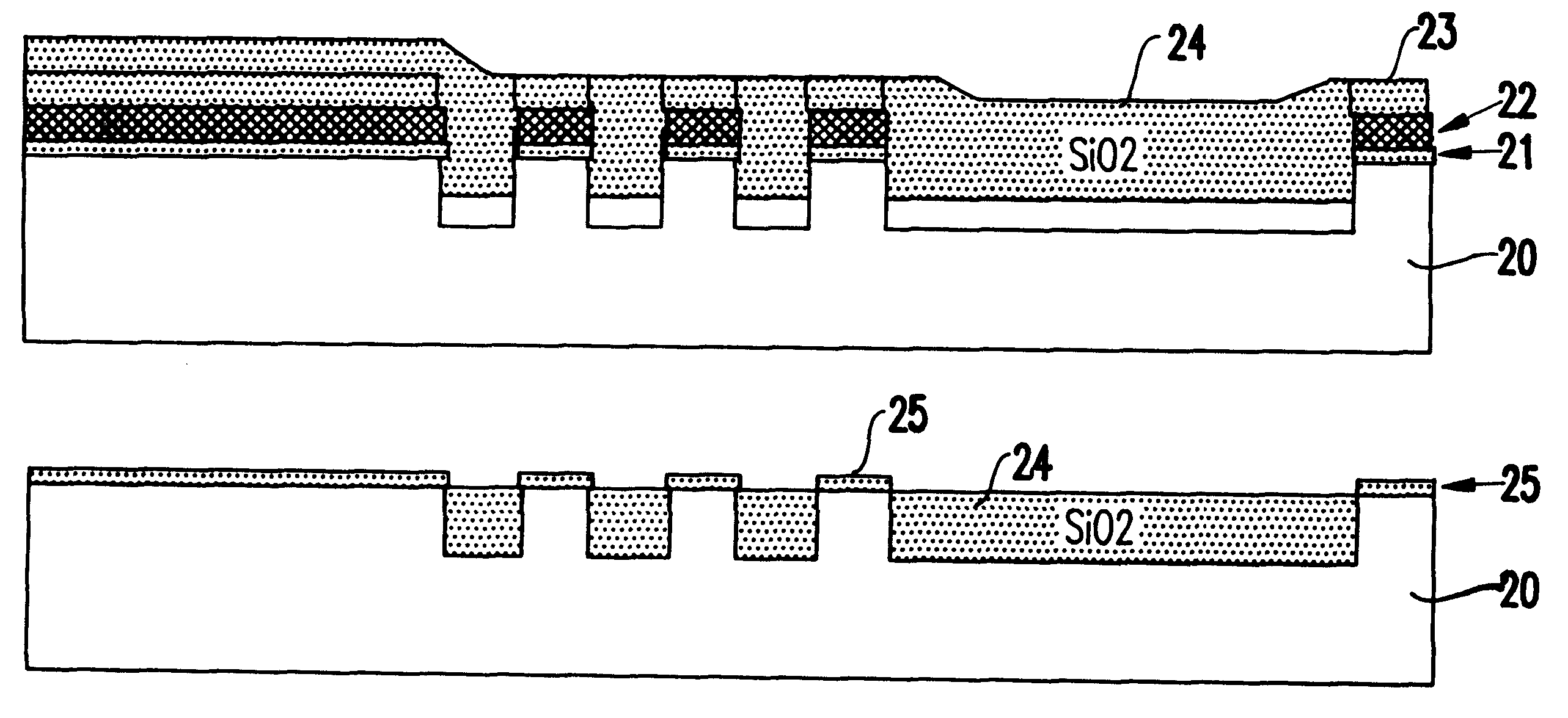
First, it is noted that the present inventors have found that use of a self-aligned layer enhances the SiO.sub.2 polish rate above the pad nitride regions (i.e., active area). This results in a faster polish rate in these regions without altering the polish rate in regions with wide trenches, thereby resulting in a thicker SiO.sub.2 layer in the wide trenches after Chemical Mechanical Polishing.

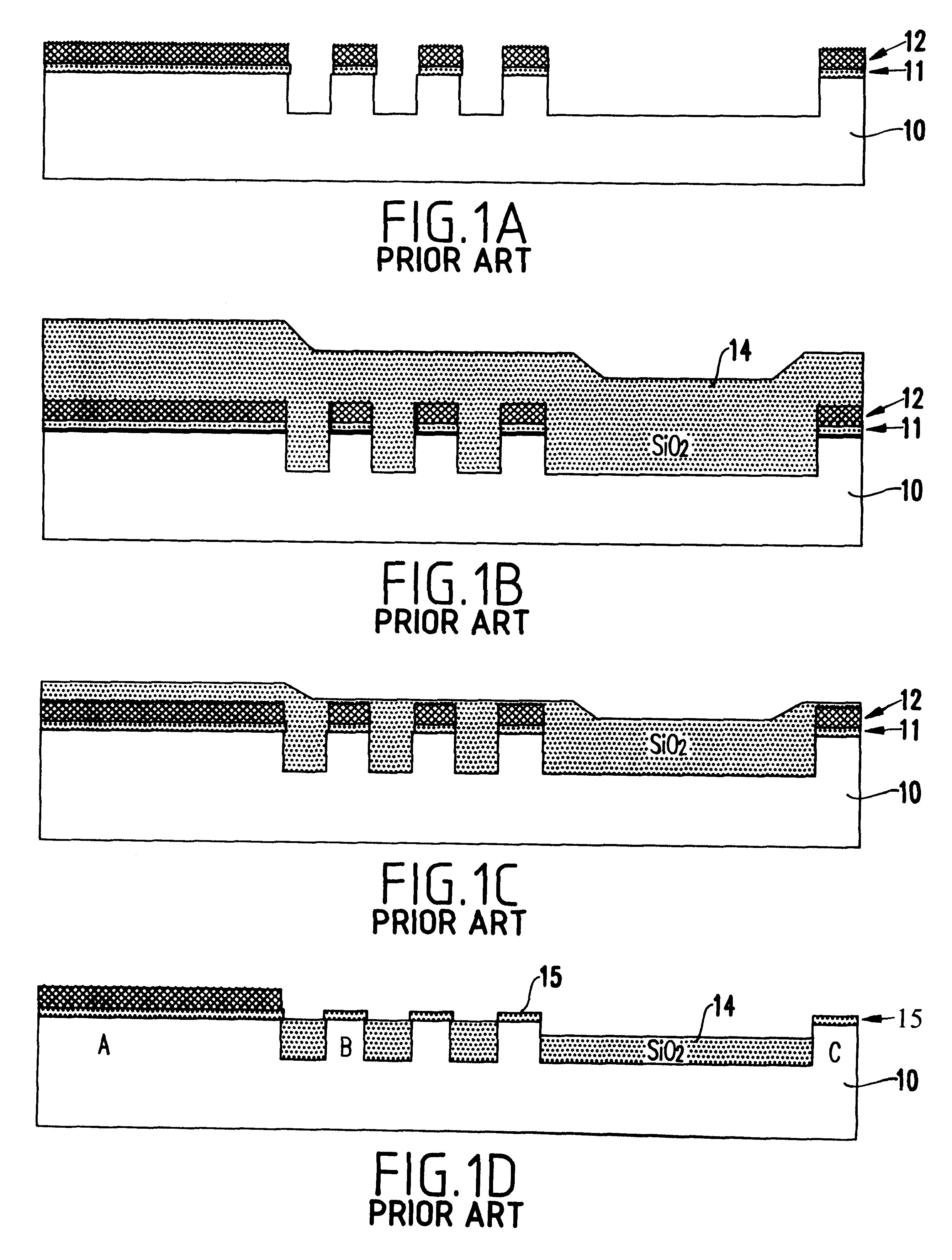
Similarly, a self-aligned layer (e.g., preferably doped SiO.sub.2 or porous SiO.sub.2) with a fast polish rate can be placed above the pad nitride so that less over-polish is required to remove the SiO.sub.2 from regions with wide active areas. A process flow according to the invention is described hereinbelow, with reference to FIGS. 2A-2D. FIG. 2E illustrates a flowchart of the process 200 of the first embodiment. The advantages of such a method will be clear especially when comparing the inventive process with the conventional process shown in FIGS. 1A-1D.

Referring to FIG. 2A, first an ins...

second embodiment

A similar approach may be used for metal Chemical Mechanical Polishing, as shown in FIGS. 4A-4C and the flowchart of the process 400 shown in FIG. 4D.

First, as a basis for comparison a conventional metal CMP will be described referring to FIGS. 3A-3C. Referring to FIG. 3A, an interlevel dielectric (ILD) 31 is deposited and then trenches 32 are etched therein.

In FIG. 3B, a titanium / titanium nitride (Ti / TiN) liner 33 is deposited in the trenches 32 along with a conductor (e.g., tungsten) 34, thereby to fill the trenches 32.

In FIG. 3C, the conductor 34 is patterned by CMP.

However, as mentioned above, in the case of metal CMP, there is generally excessive removal of metal in regions with wide metal features (e.g., see region C in FIG. 3C), whereas there may be insufficient removal of metal in wide oxide regions (e.g., see region A in FIG. 3C). The excessive thinning of metal results in high resistance, and increased circuit delays. The residual metal on top of the dielectric 31 (see Reg...

third embodiment

According to a third embodiment of the present invention, this approach also can be used for oxide CMP over a gate stack, where the gate stack is used as a polish stop, as shown in FIGS. 6A-6C.

First, a conventional method of oxide CMP over a gate stack is shown in FIGS. 5A-5D.

First, in FIG. 5A, over a silicon substrate 50 is formed a SiO.sub.2 layer 51, a polysilicon 52 and a SiN layer 53 in turn. The gate stack is patterned, as shown.

In FIG. 5B, a dielectric 54 is deposited.

In FIG. 5C, the dielectric 54 is patterned by CMP.

To improve over the conventional process of FIGS. 5A-5C, in the third embodiment, a self-aligned layer 65 of doped SiO.sub.2 or porous SiO.sub.2 is used to enhance the SiO.sub.2 polish rate above the wide gate regions. This results in a faster polish rate in these regions without altering the polish rate in regions with wide trenches, thereby resulting in a thicker SiO.sub.2 layer in the wide trenches after CMP. A process flow is described below with reference to...


PUM

PropertyMeasurementUnit
thicknessaaaaaaaaaa
thicknessaaaaaaaaaa
thicknessaaaaaaaaaa

Abstract

A method for making a semiconductor device, includes forming an oxide layer on a silicon substrate, forming a nitride layer over the oxide layer; depositing one of a doped oxide layer and an undoped porous oxide layer on the nitride layer, etching trenches through the one of the doped layer and the undoped porous oxide layer, the nitride layer, and the oxide layer, depositing an undoped oxide layer to fill the trenches, and patterning the undoped oxide by chemical mechanical polishing (CMP).

Description

1. Field of the InventionThe present invention generally relates to a method for producing a semiconductor device, and more particularly to a method for improving uniformity of a chemical mechanical polishing (CMP) operation used in producing the semiconductor device.2. Description of the Related ArtConventional systems utilize shallow trench isolation (STI) in advanced integrated circuits to electrically isolate neighboring devices. Chemical mechanical polishing (CMP) is often used to pattern insulators in semiconductor trenches or conductors in insulating trenches. In many applications, the polishing is stopped only after all the material has been removed from the field regions.However, oftentimes this operation results in over-polishing of the material in wide trenches.For example, FIGS. 1A-1D illustrate a conventional process which is relatively simple, and is extendable to sub-quarter micron dimensions. In FIG. 1A, a pad oxide 11 is grown by thermal oxidation of a silicon subst...

Claims


Application Information

Patent Timeline
Patent Type & Authority Patents(United States)
IPC IPC(8): H01L21/762H01L21/70H01L21/02H01L21/3105
CPCH01L21/76229H01L21/31053
Inventor DIVAKARUNI, RAMACHANDRAGAMBINO, JEFFREY PETERRADENS, CARL J.STEPHENS, JEREMY K.
Owner IBM CORP
Why Eureka
Try Eureka