Selective growth process for group III-nitride-based semiconductors

Inactive Publication Date: 2001-07-24
AVAGO TECH INT SALES PTE LTD
View PDF15 Cites 33 Cited by
  • Summary
  • Abstract
  • Description
  • Claims
  • Application Information

AI Technical Summary

Benefits of technology

In a preferred embodiment of the present invention, the GaN is plasma deposited using a reactive nitrogen species. This process results in the required vertical growth of the GaN film over both the substrate and masking layer. The polycrystalline GaN film will include both N-polar and Ga-polar surfaces, while the single crystal material will exhibit only Ga-polar faces. In order to etch away the polycrysta

Problems solved by technology

One of the drawbacks of reactive ion etching includes the generation of ion-induced damage on the surface of the GaN film.
In particular, the etch rates have been too slow for efficient processing.
Further, the wet etch techniques have generally not been directional enough to produce sidewalls that mirror the masking material.
In

Method used


Image

  • Selective growth process for group III-nitride-based semiconductors
  • Selective growth process for group III-nitride-based semiconductors

Examples


Embodiment Construction

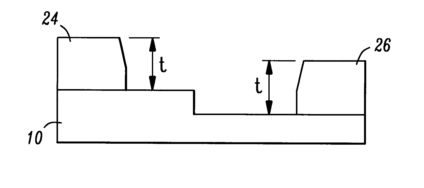
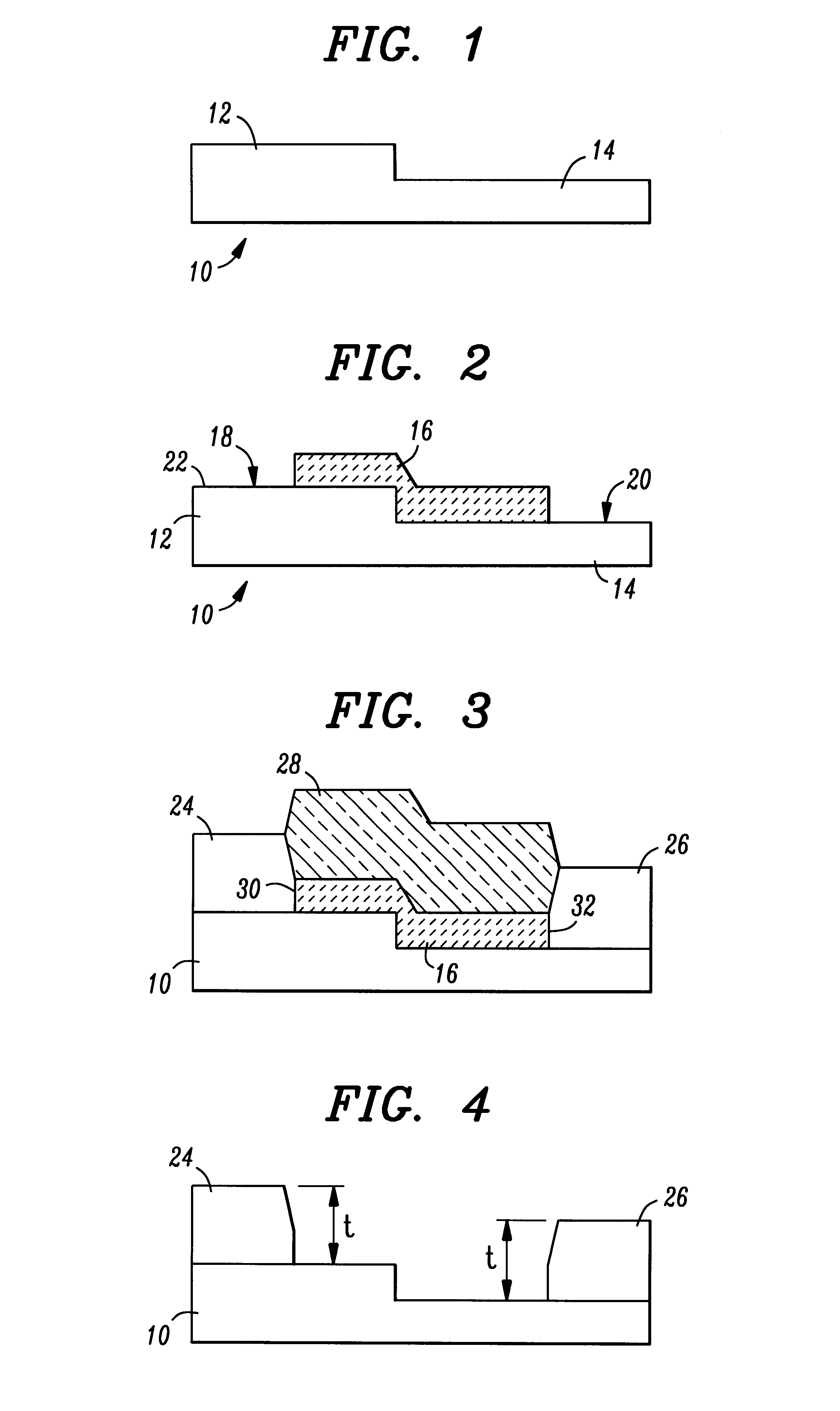
FIG. 1 illustrates, in a cross-sectional view, an exemplary substrate 10 that can be processed in accordance with the present invention to provide selective growth of a Group III-nitride film. Substrate 10 can comprise a variety of materials, including but not limited to, Al.sub.2 O.sub.3, SiC and GaN. Further, substrate 10 does not necessarily need to be planar. Indeed, as illustrated in FIG. 1, exemplary substrate 10 is formed to include a first region 12 that is raised above a second region 14. In general, the process of the present invention relates to forming a selective Group III-nitride layer on the exposed surface of substrate 10. For the purposes of the present discussion, the formation of a selective GaN film will be discussed, although it is to be understood that various other Group III-nitrides can similarly be formed.

Referring to FIG. 2, the initial step in the process of the present invention is to form a masking layer 16 that is patterned to leave exposed those areas ...


PUM


Abstract

A method of forming selected Group III-nitride regions uses a masking layer to cause differential growth between single crystal Group III-nitride material and polycrystalline Group III-nitride material. The epitaxial process is chosen to provide vertical growth so as to allow for replication of the mask edges at the defined limits for the selected regions. By using an etchant that is selective between polycrystalline and single crystal Group III-nitride material, the polycrystalline material (that grew over the mask layer) can be removed, leaving only the single crystal Group III-nitride (that grew over the exposed substrate material).

Description

TECHNICAL FIELDThe present invention relates to a selective growth technique for Group III-nitride materials and, more particularly, to the use of masking technique to form both polycrystalline and single crystal Group III-nitride films that can be preferentially processed to form selected growth areas.BACKGROUND OF THE INVENTIONGroup III nitrides, in particular, GaN, are of interest for many electronic and optoelectronic applications, including high temperature electronic devices, high-power microwave circuits, blue lasers and LEDs, as well as solar-blind photodetectors. For these applications, the semiconductor layers are grown epitaxially on a crystalline substrate. After the epitaxial growth, a masking layer is typically deposited on the surface and lithographically patterned. The pattern can then be transferred to the underlying semiconductor material by etching. There are several reasons why this patterning is needed, including device isolation, contact to underlying layers, a...

Claims


Application Information

Patent Timeline
IPC IPC(8): H01L21/02H01L21/20H01L21/318C30B29/38H01L21/205H01L21/308
CPCH01L21/3185H01L21/02639H01L21/0254H01L21/0237H01L21/0217
Inventor ANSELM, KLAUS ALEXANDERCHO, ALFRED YICHU, SUNG-NEE GEORGE
Owner AVAGO TECH INT SALES PTE LTD
Why Eureka
Try Eureka