Monolithic ceramic electronic component

a technology of electronic components and monolithic ceramics, applied in the direction of fixed capacitor details, fixed capacitors, natural mineral layered products, etc., can solve the problems of high material cost, difficult to reduce product cost, and high cost of electrode materials

Inactive Publication Date: 2001-08-07
MURATA MFG CO LTD
View PDF14 Cites 18 Cited by
  • Summary
  • Abstract
  • Description
  • Claims
  • Application Information

AI Technical Summary

Problems solved by technology

However, these electrode materials are very expensive, and the material cost occupied a large part of the product cost.
Thus, it was difficult to reduce the product cost.
However, since the particle size is large, it is difficult to form the thin inner electrodes.
However, if the ceramic layer has a thickness of 3 .mu.m or less when the inner electrodes each have a thickness of 0.8 .mu.m, delamination is often caused due to the difference in shrinkage between the inner electrode material and the ceramic.
This is one of fatal defects of the monolithic ceramic capacitors.
When the powders are baked, this causes the problem that the coverage (effective electrode areas) of the inner electrodes is reduced (with an increase in the frequency of electrode breaking).
Thus, this brings the reduction in reliability of the monolithic ceramic capacitor.
Thus, the inner electrodes can not achieve their functions.
If the mean particle size of the Ni powder is less than about 10 nm, it is difficult to prepare the paste having a viscosity applicable for the printing such as screen printing.
Defects of "scratching" and pinholes are caused, which may bring the reduction of the coverage and the electrode breaking.

Method used


Image

  • Monolithic ceramic electronic component
  • Monolithic ceramic electronic component
  • Monolithic ceramic electronic component

Examples


Embodiment Construction

Hereinafter, the present invention will be described with reference to specific examples in detail. It is to be understood that the practicable mode of the present invention, not departing from the scope of the present invention, is not restricted on the following example. For example, as dielectric ceramics in the example, only a barium titanate type is exemplified. However, it has been demonstrated that the same advantages as those of the barium titanate type can be obtained by use of dielectric ceramics having a perovskite-type structure and containing as a major component strontium titanate, calcium titanate, and the like.

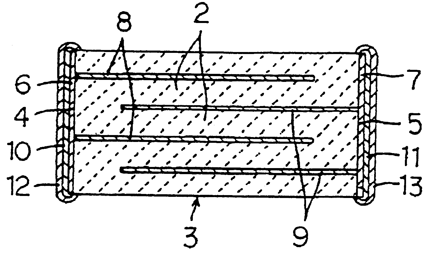
A monolithic ceramic capacitor 1 having such a structure as shown in FIG. 1 was prepared in the example.

1. Preparation of Sample

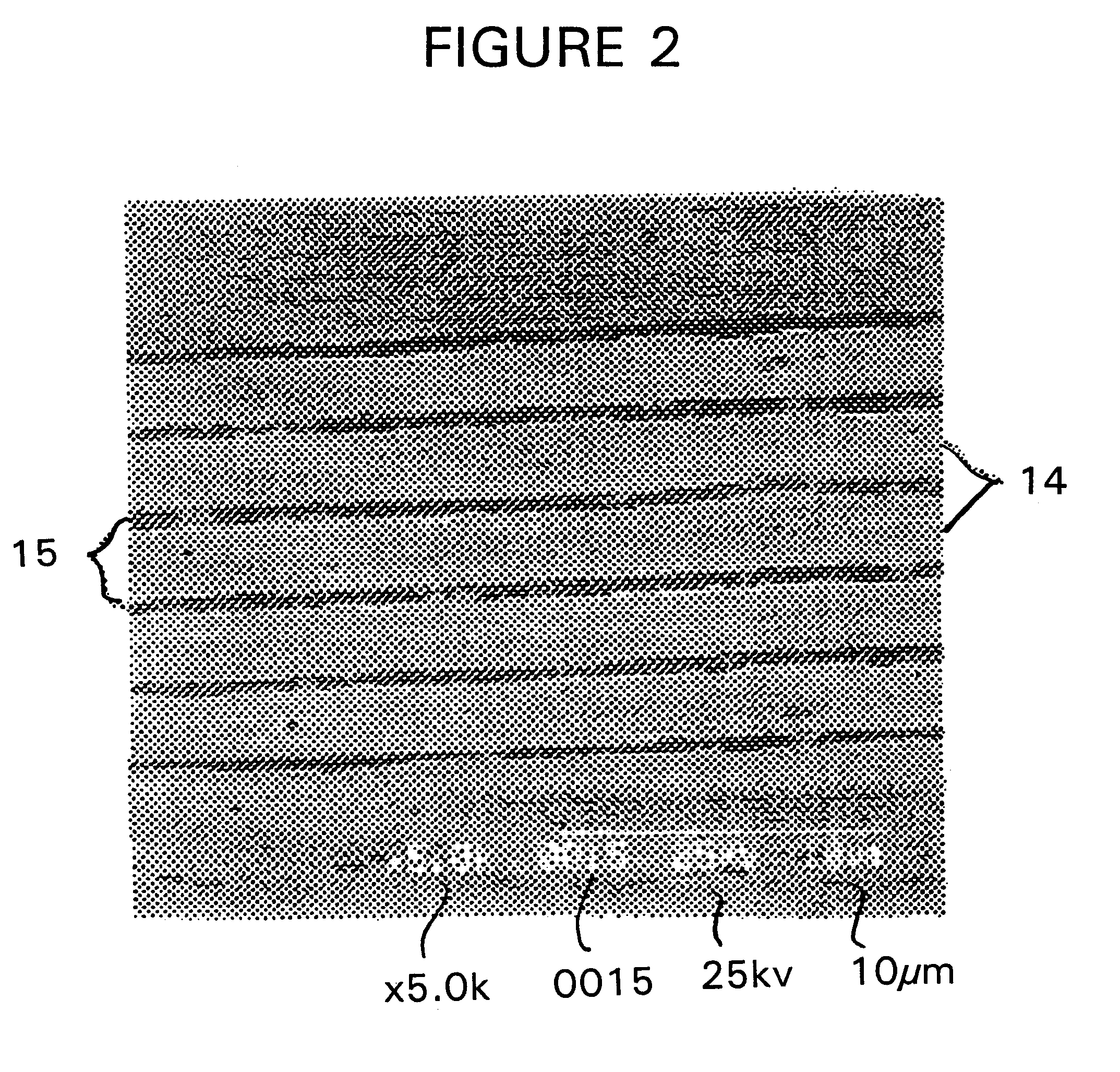
First, barium titanate (BaTiO.sub.3) powder as the ceramic raw material powder was prepared by the hydrolyzation method. The BaTiO.sub.3 powder was calcined at different calcination temperatures listed in Table 1 to prepare types of (B...


PUM

PropertyMeasurementUnit
thicknessaaaaaaaaaa
mean particle sizeaaaaaaaaaa

Abstract

A monolithic ceramic component has inner electrodes which are thin having a thickness of from about 0.2 mum to 0.7 min, and thereby, delamination is inhibited even though ceramic layers are thin, having a thickness up to about 3 mum. The mean particle size of the ceramic grains of the ceramic layers is up to 0.5 mum, so that the concavities and convexities at the interfaces between the inner electrodes and the ceramic layers can be reduced. Preferably, metal powder in a paste used to form the inner electrodes has a mean particle size of from about 10 to 200 nm, and thereby, the metal filling ratio and the smoothness of the inner electrodes can be enhanced, and the coverage can be improved.

Description

1. Field of the InventionThe present invention relates to a monolithic ceramic electronic component such as a monolithic ceramic capacitor, and more particularly to an improvement in an inner electrode of the same.2. Description of the Related ArtConventionally, dielectric ceramic materials such as barium titanate, strontium titanate, calcium titanate, and the like, having a perovskite-type structure have been widely used as capacitor materials, due to their high dielectric constants. With the recent tendency that electronic components are small-sized, capacitors, which are passive components, are required to have a high electrostatic capacitance and also to be miniaturized.For monolithic ceramic capacitors containing ceramic dielectric materials in their dielectric layers, it is necessary to bake the dielectric ceramic materials at high temperatures, for example, at about 1300.degree. C. in the atmosphere. Therefore, as the inner electrodes, noble metals such as palladium, platinum...

Claims


Application Information

Patent Timeline
Patent Type & Authority Patents(United States)
IPC IPC(8): H01G4/30H01G4/12H01G4/008
CPCH01G4/30H01G4/0085H01G4/12
Inventor NAKAMURA, TAKANORIYAMANA, TSUYOSHIWADA, NOBUYUKIMIYAZAKI, TAKAHARU
Owner MURATA MFG CO LTD
Why Eureka
Try Eureka