

Method of making an SRAM cell and structure
a sram cell and sram technology, applied in the direction of semiconductor devices, electrical apparatus, transistors, etc., can solve the problems of reducing the overall cell size, the area of the cell, and the need for a larger footprint for speed and stability
- Summary
- Abstract
- Description
- Claims
- Application Information
AI Technical Summary
Benefits of technology
Problems solved by technology
Method used
Image

Examples
Embodiment Construction
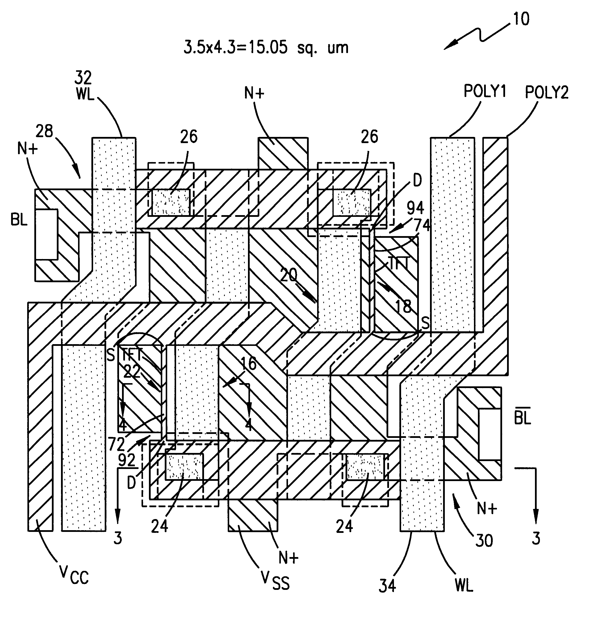
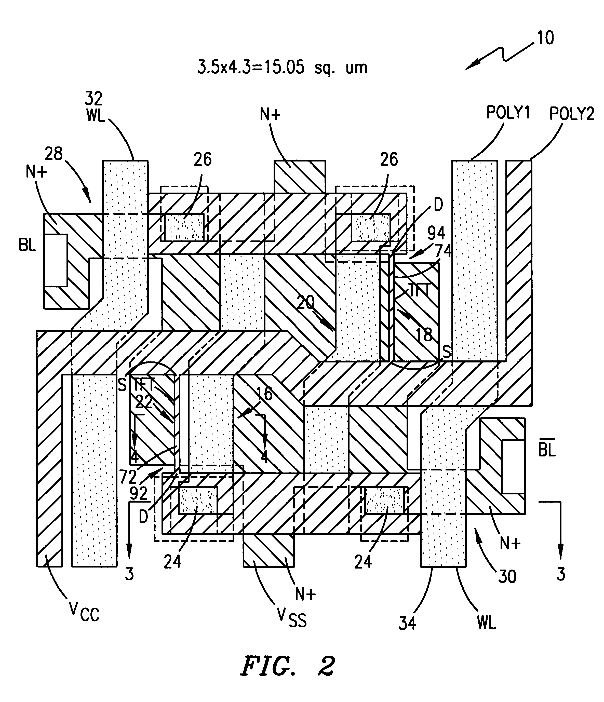
The process steps and structures described herein do not form a complete process flow for manufacturing integrated circuits. The present invention can be practiced in conjunction with integrated circuit fabrication techniques currently used in the prior art, and only so much of the commonly practiced process steps are included as are necessary for an understanding of the present invention. The figures representing portions of an integrated circuit during fabrication are not drawn to scale but instead are drawn so as to illustrate the important features of the invention.
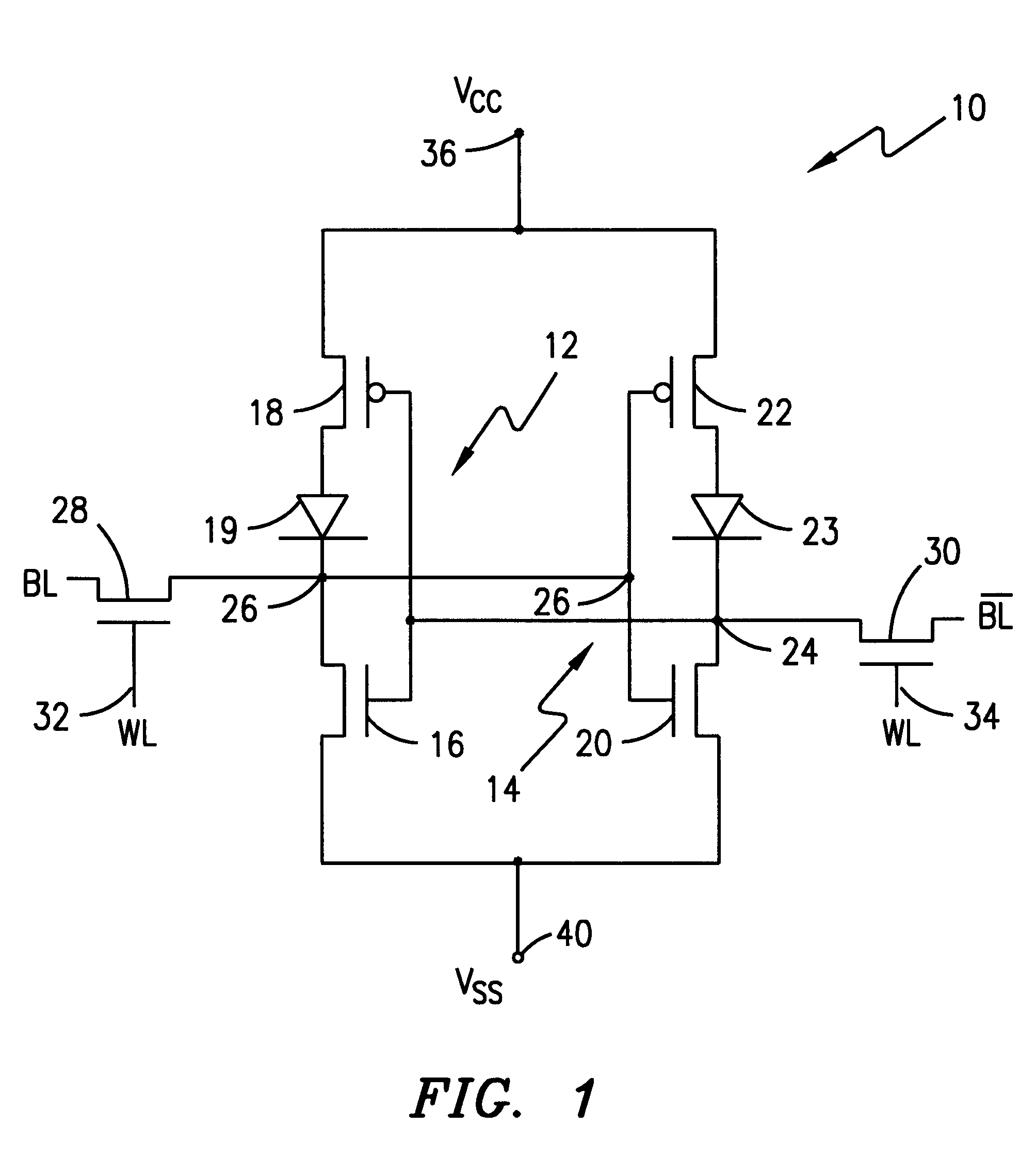
Referring now to FIG. 1, a schematic circuit diagram of an SRAM cell 10 according to the present invention is shown. Memory cell 10 is further illustrated in an MOS integrated circuit layout in accordance with the invention in FIG. 2. Memory cell 10 includes two cross-coupled, CMOS inverters 12 and 14. CMOS inverter 12 includes an NMOS driver transistor 16 and a PMOS thin-film, load transistor 18 fabricated in accorda...
PUM
 Abstract
Description
Claims
Application Information