

Merged logic and memory combining thin film and bulk Si transistors
a logic and memory technology, applied in the direction of transistors, semiconductor devices, electrical equipment, etc., can solve the problems of limiting the overall system speed by the communication bandwidth between logic and memory, and the performance limit of about 500 mhz
- Summary
- Abstract
- Description
- Claims
- Application Information
AI Technical Summary
Benefits of technology
Problems solved by technology
Method used
Image

Examples
Embodiment Construction
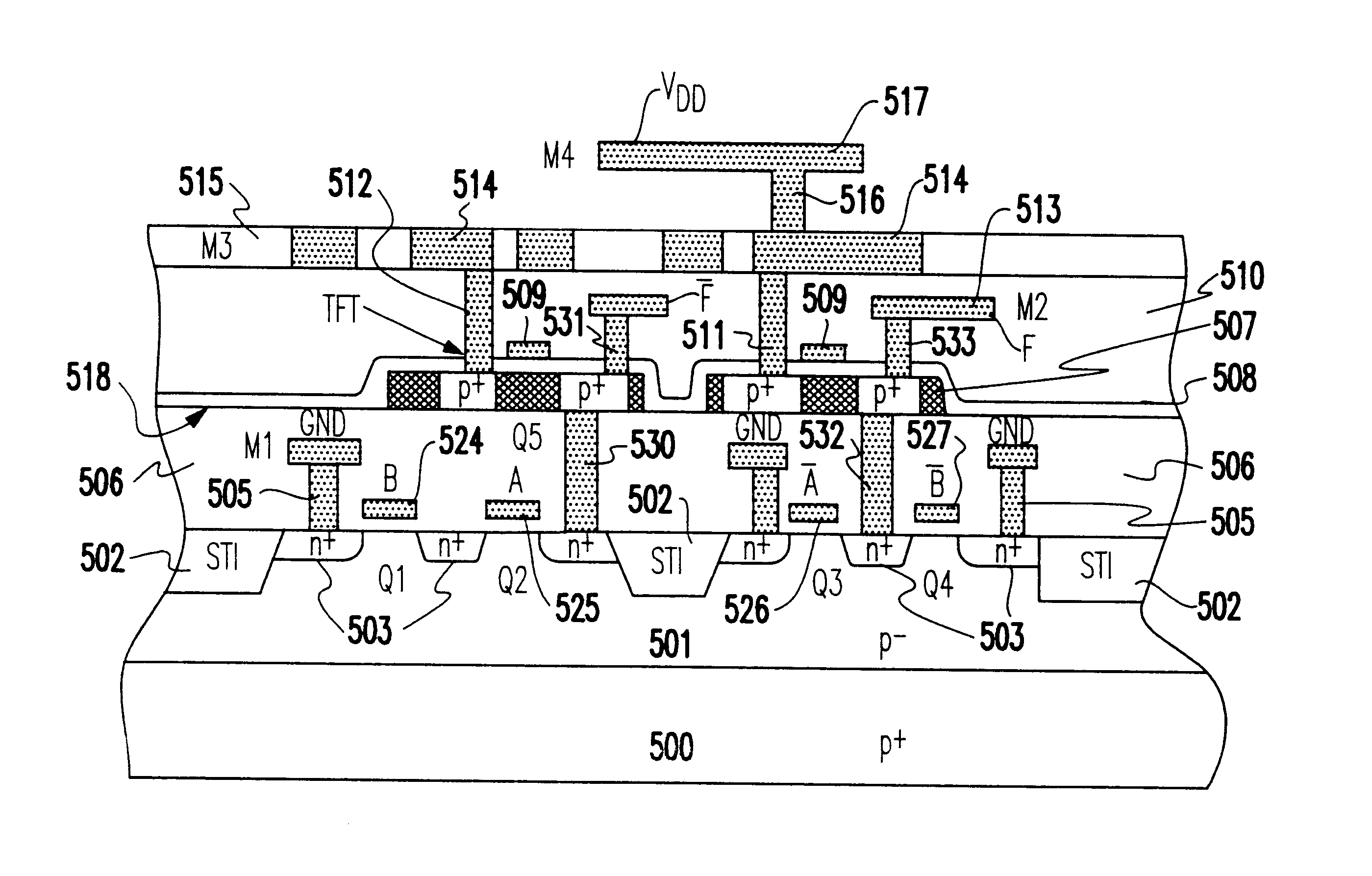
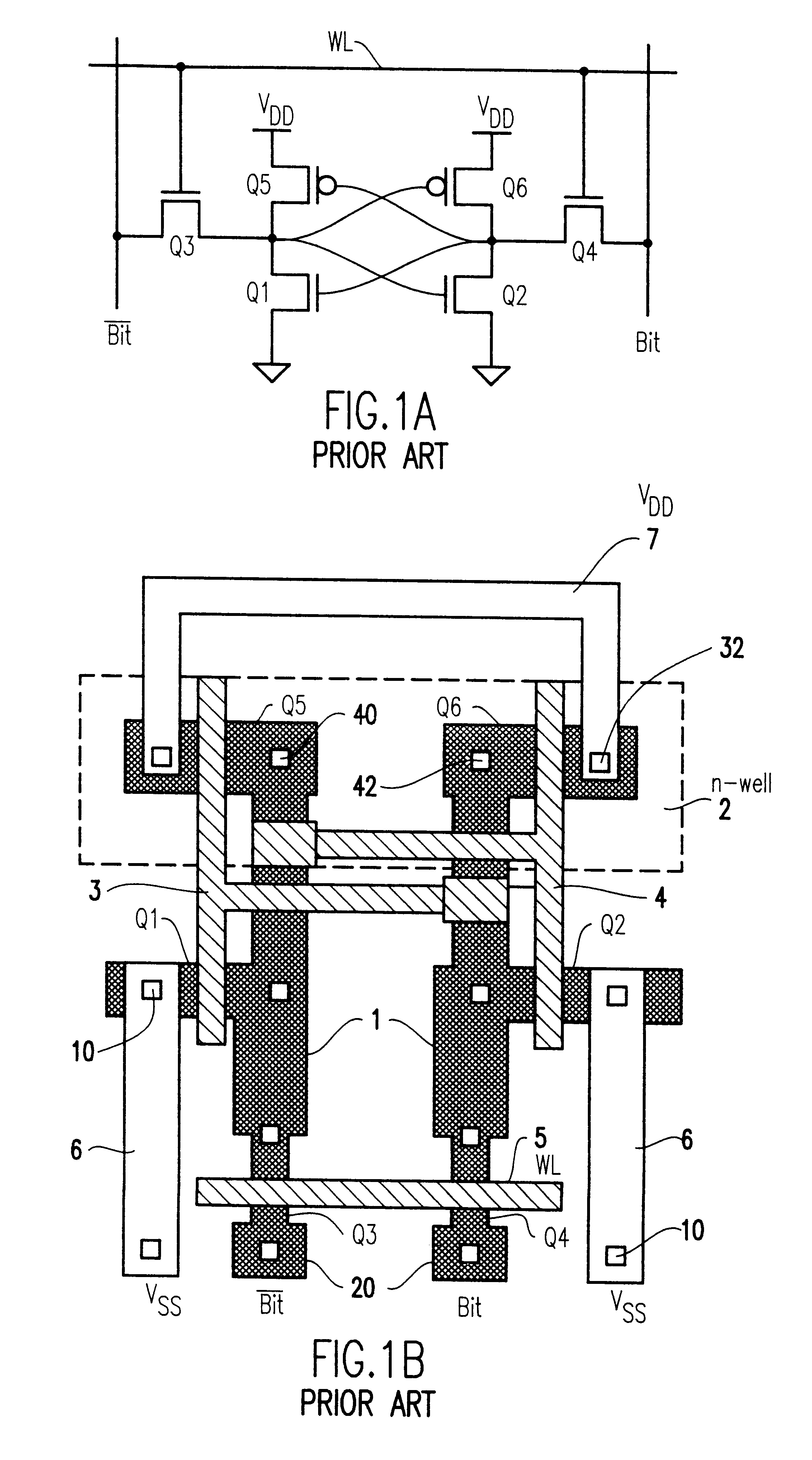
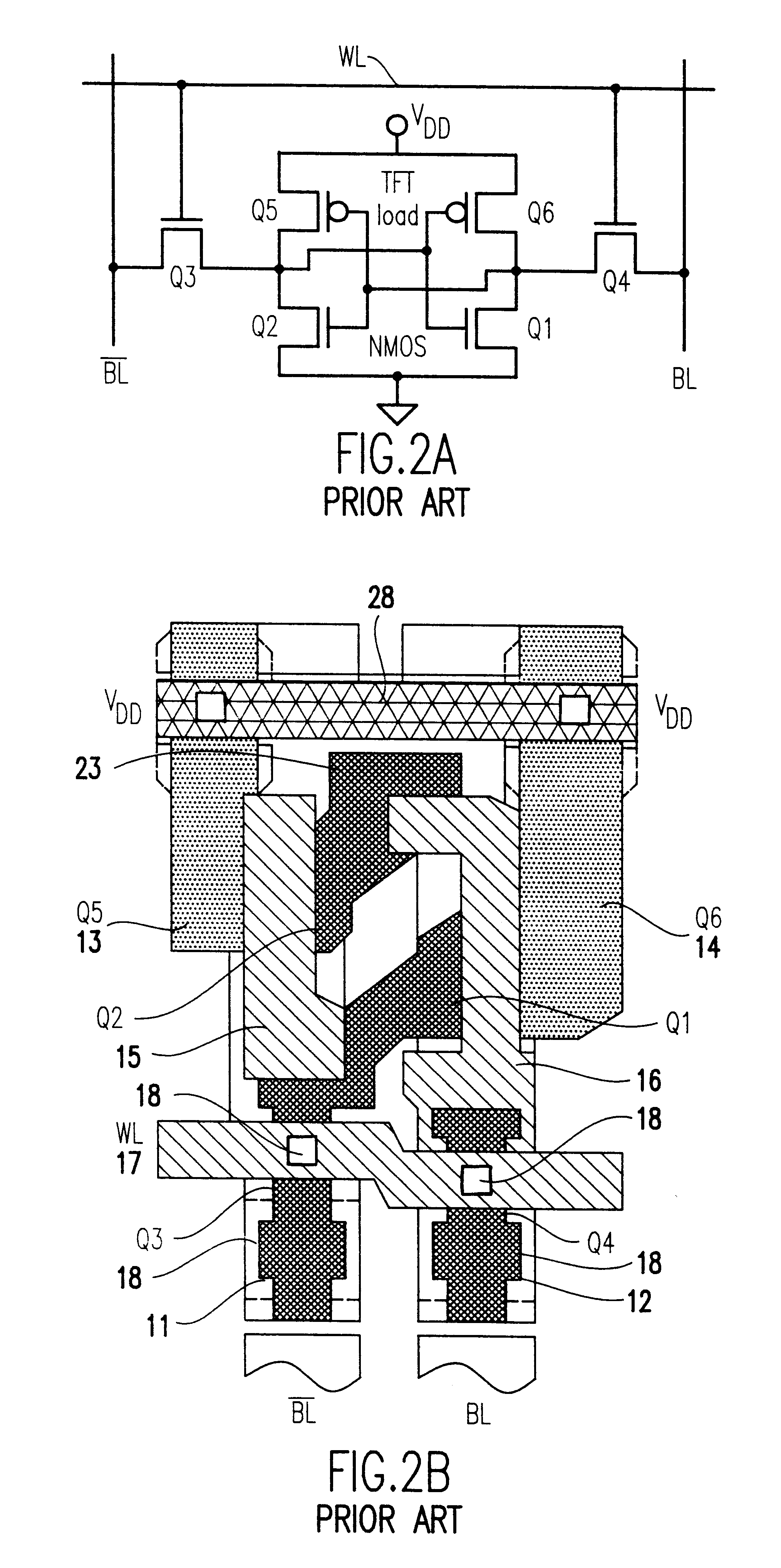
Referring now to the drawings, and more particularly to FIGS. 1A and 1B, there is shown an example of the prior art of a planar static random access memory (SRAM) arrays. FIG. 1A is a schematic circuit diagram illustrating a standard six transistor CMOS SRAM cell. The NMOS transistors Q1 and Q2 are the "access" devices, the NMOS transistors Q3 and Q4 are "driver" transistors, and the two PMOS transistors Q5 and Q6 are "load" transistors.
The layout plan view of a standard SRAM cell is shown in FIG. 1B. Q1 and Q2 NMOS transistors are formed by the overlap of the active n-silicon 1 and polysilicon layers 3 and 4. The source contacts 10 of Q1 and Q2 are contacted by metal layer 6 to V.sub.ss or ground. Similarly, Q3 and Q4 are formed by overlap of the active silicon 31 and polysilicon layer 5 which forms the word line (WL). The drain contacts 20 of Q3 and Q4 are connected to bitlines Bit and Bit, respectively. The PMOS Q5 and Q6 transistors are connected to metal layer 7 to V.sub.DD. Th...
PUM
 Abstract
Description
Claims
Application Information