CVD apparatus for forming thin films using liquid reaction material

a technology of liquid reaction material and cvd apparatus, which is applied in mechanical apparatus, combustion-air/fuel-air treatment, machines/engines, etc., can solve the problem of high risk of creating a source of particle generation

Inactive Publication Date: 2001-08-21
ASM JAPAN
View PDF8 Cites 46 Cited by
  • Summary
  • Abstract
  • Description
  • Claims
  • Application Information

AI Technical Summary

Problems solved by technology

This will create the source of particle generation and will contaminate semiconductor substrates in the subsequent thin

Method used


Image

  • CVD apparatus for forming thin films using liquid reaction material
  • CVD apparatus for forming thin films using liquid reaction material
  • CVD apparatus for forming thin films using liquid reaction material

Examples


Embodiment Construction

This invention is explained referring to the drawings in the following:

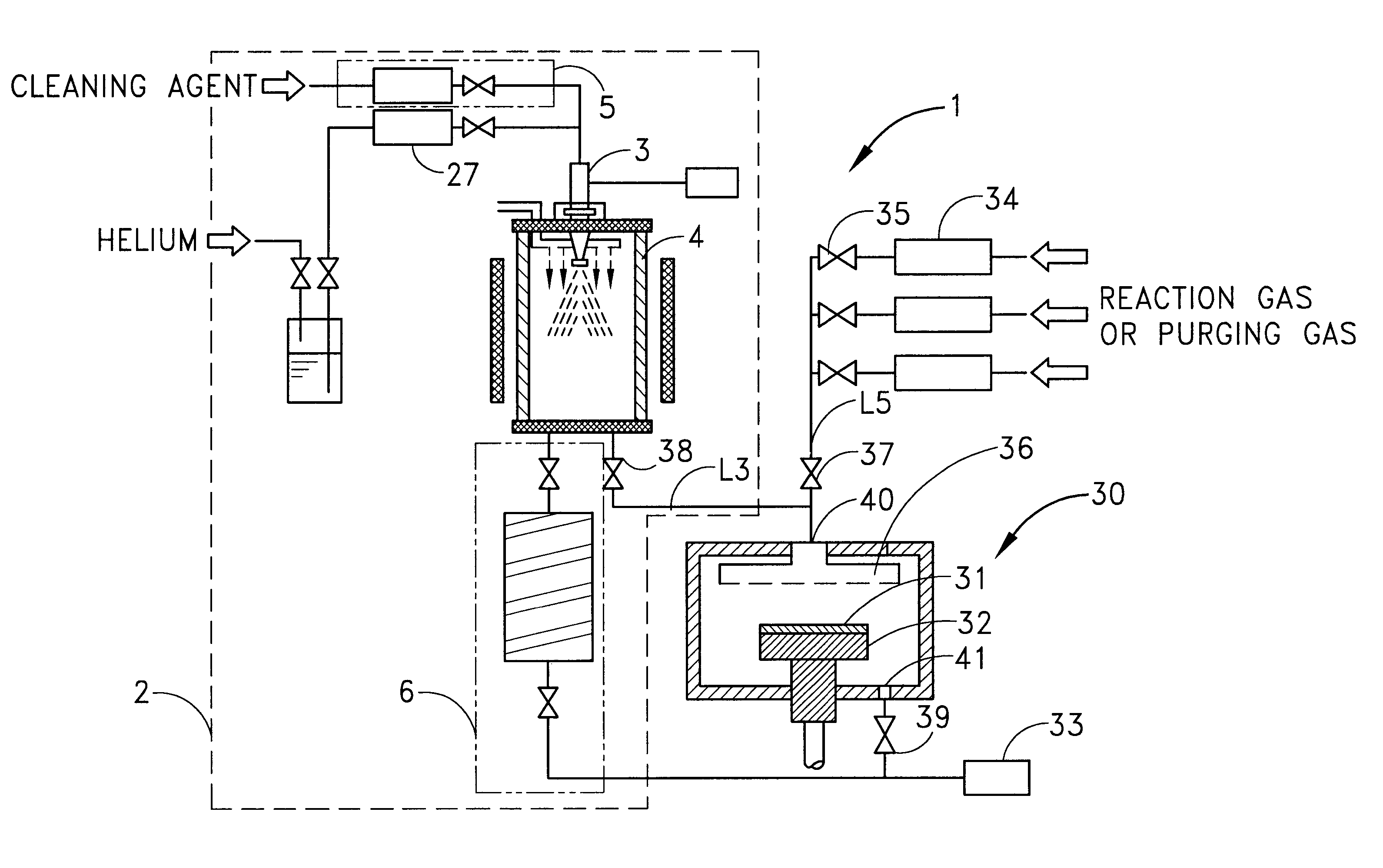
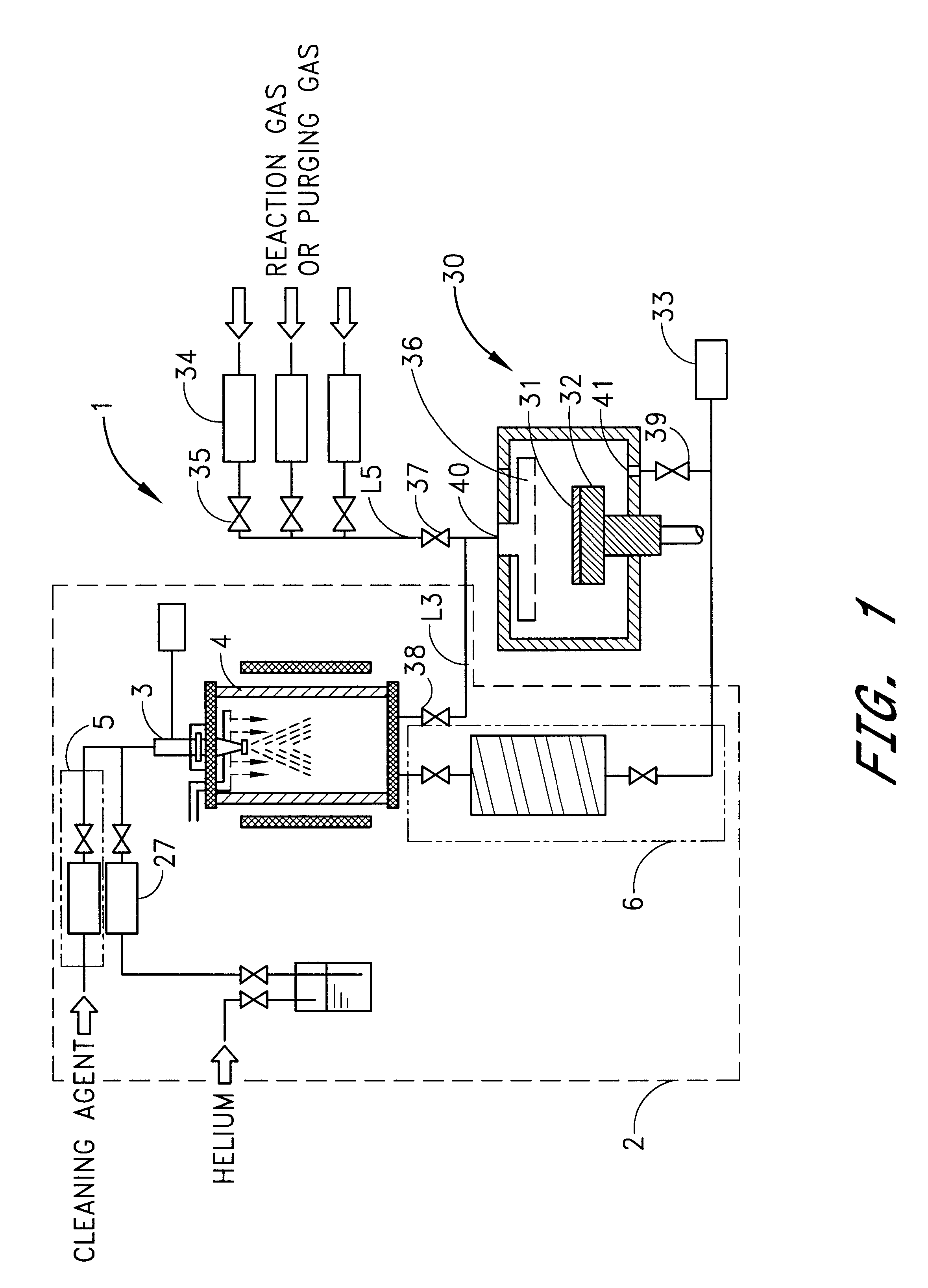
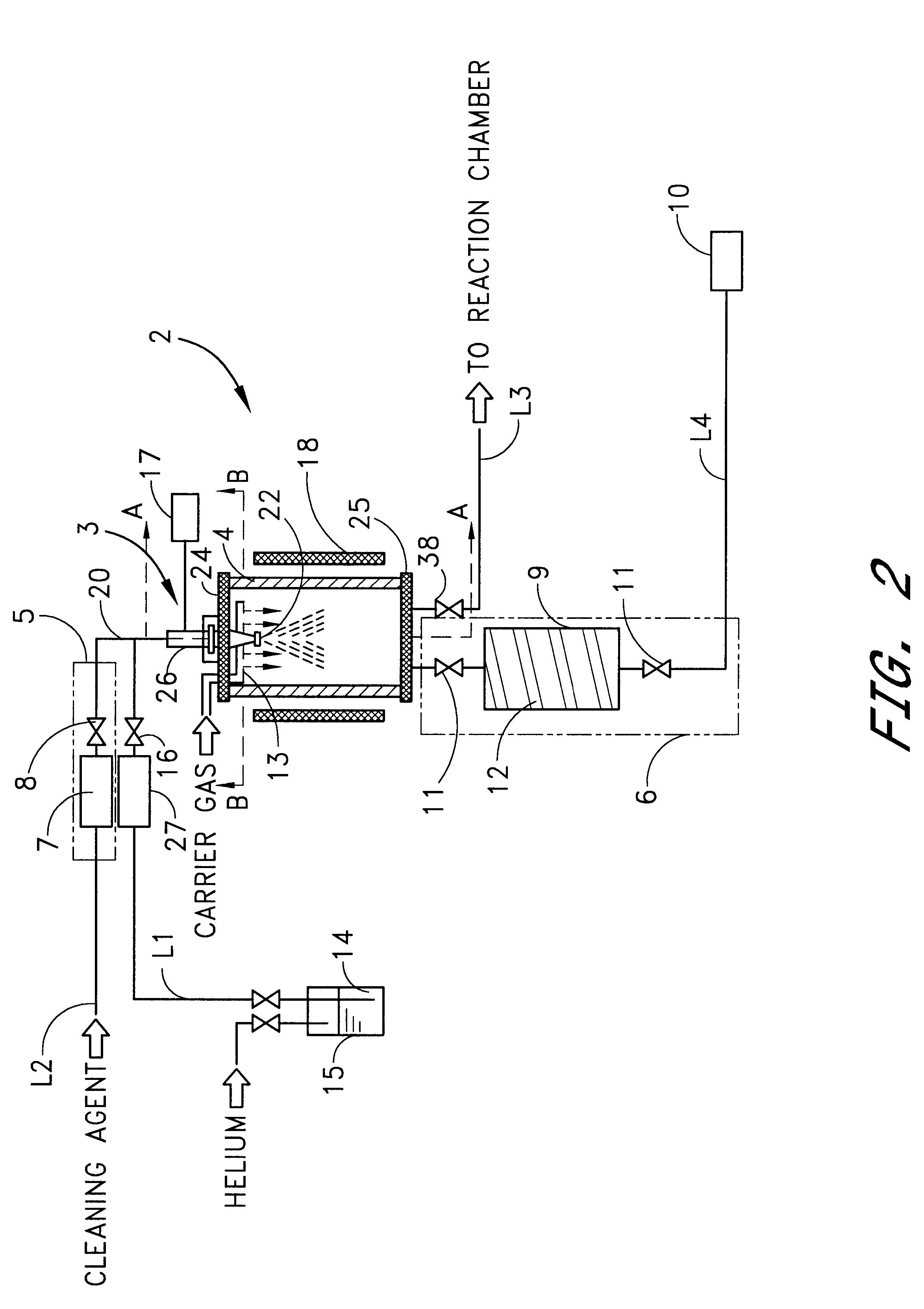
FIG. 1 schematically illustrates a suitable implementation example of the CVD apparatus according to the invention. The CVD apparatus (1) according to the invention comprises a reaction chamber (30), a vacuum exhaust device (33) that is connected to the reaction chamber (30) and which vacuums and exhausts the reaction chamber (30), a susceptor (32) that is provided within the reaction chamber (30) and maintains a semiconductor substrate (31), a showerhead (36) that is set up on the susceptor (32) and supplies a reaction gas to the surface of the semiconductor substrate (31), and a liquid-source vaporization system (2) that is connected to the showerhead (36) and vaporizes a liquid reaction material by controlling its flow rate to supply it into the reaction chamber (30). In the above, other types of reaction gas supplier can be substituted for the showerhead. The reaction gas supplier may include reaction gas noz...


PUM

PropertyMeasurementUnit
Pressureaaaaaaaaaa
Flow rateaaaaaaaaaa
Semiconductor propertiesaaaaaaaaaa

Abstract

A CVD apparatus includes: (a) a reaction chamber; (b) a vacuum device connected to the reaction chamber for vacuuming and exhausting the reaction chamber; (c) a susceptor that maintains the semiconductor substrate inside the reaction chamber; (d) a reaction gas supplier that supplies a reaction gas to the surface of the semiconductor substrate set on the susceptor; and (e) a liquid-source vaporization system connected to the reaction gas supplier, which is disposed upstream of the showerhead and is used for atomizing and vaporizing the liquid reaction material at a given flow rate prior to its entry into the reaction chamber. The liquid-source vaporization system includes: (i) an atomizer connected to a liquid reaction material supply source; and (ii) a vaporizer connected to the atomizer downstream thereof.

Description

1. Field of the InventionThis invention relates to a CVD (Chemical Vapor Deposition) apparatus to form a thin film on a semiconductor substrate by a CVD method using liquid reaction materials having a low vapor pressure. Particularly, it relates to the CVD apparatus with a liquid-source vaporization system that supplies a flow-controlled liquid reaction material after its vaporization.2. Description of the Related ArtUp to this time, the CVD method has been widely adopted as a thin film formation method for a semiconductor apparatus. The CVD method is a method to form a thin film on a substrate by importing several types of gases selected according to the type of film to be formed into the reaction chamber and causing a chemical reaction by applying thermal energy or plasma excitation energy. In recent years, liquid reaction materials with low vapor pressure have attracted more attention for the reasons that they are excellent in covering and filling gaps or steps.For example, Japan...

Claims


Application Information

Patent Timeline
IPC IPC(8): C23C16/44C23C16/448C23C16/455H01L21/205
CPCC23C16/4486C23C16/4405
Inventor NISHIKAWA, TOMOHISA
Owner ASM JAPAN
Why Eureka
Try Eureka