Multistack 3-dimensional high density semiconductor device and method for fabrication

a semiconductor device and multi-layer technology, applied in semiconductor devices, semiconductor/solid-state device details, electrical apparatus, etc., can solve the problems of power consumption, limited integration that can be achieved on semiconductor chips, and limited performance of a system which is realized using planar technology and comprises a plurality of chips connected to one another, so as to improve the function, density and performance of the device.

Inactive Publication Date: 2001-09-18
IBM CORP
View PDF14 Cites 74 Cited by
  • Summary
  • Abstract
  • Description
  • Claims
  • Application Information

AI Technical Summary

Benefits of technology

The present invention provides for a multistack three-dimensional semiconductor structure that does not require the precision alignment of prior art devices. Moreove

Problems solved by technology

The level of integration that can be achieved on a semiconductor chip is limited by the size of the chip and by the structural fineness that is obtainable.
The performance of a system which is realized using planar technology and which comprises a plurality of chips connected to one another is restricted by the number of possible connections between individual chips via connection contacts, the signal transmission speed that can be achieved via such connections (the so-called frequency performance) and also by the power consumption.
The components produced in the substrate prior to the deposition of the further semiconductor are exposed during the recrystallization step to the thermal loading associated with the laser annealing, which leads to a very limited yield for the chips due to large numbers of defects which typically occur.
This has the disadvantage that the thinned wafers have to be processe

Method used


Image

  • Multistack 3-dimensional high density semiconductor device and method for fabrication
  • Multistack 3-dimensional high density semiconductor device and method for fabrication
  • Multistack 3-dimensional high density semiconductor device and method for fabrication

Examples


Embodiment Construction

In order to facilitate an understanding of the present invention, reference may be made to the figures which illustrate a diagrammatic representation of the steps of an embodiment according to the present invention.

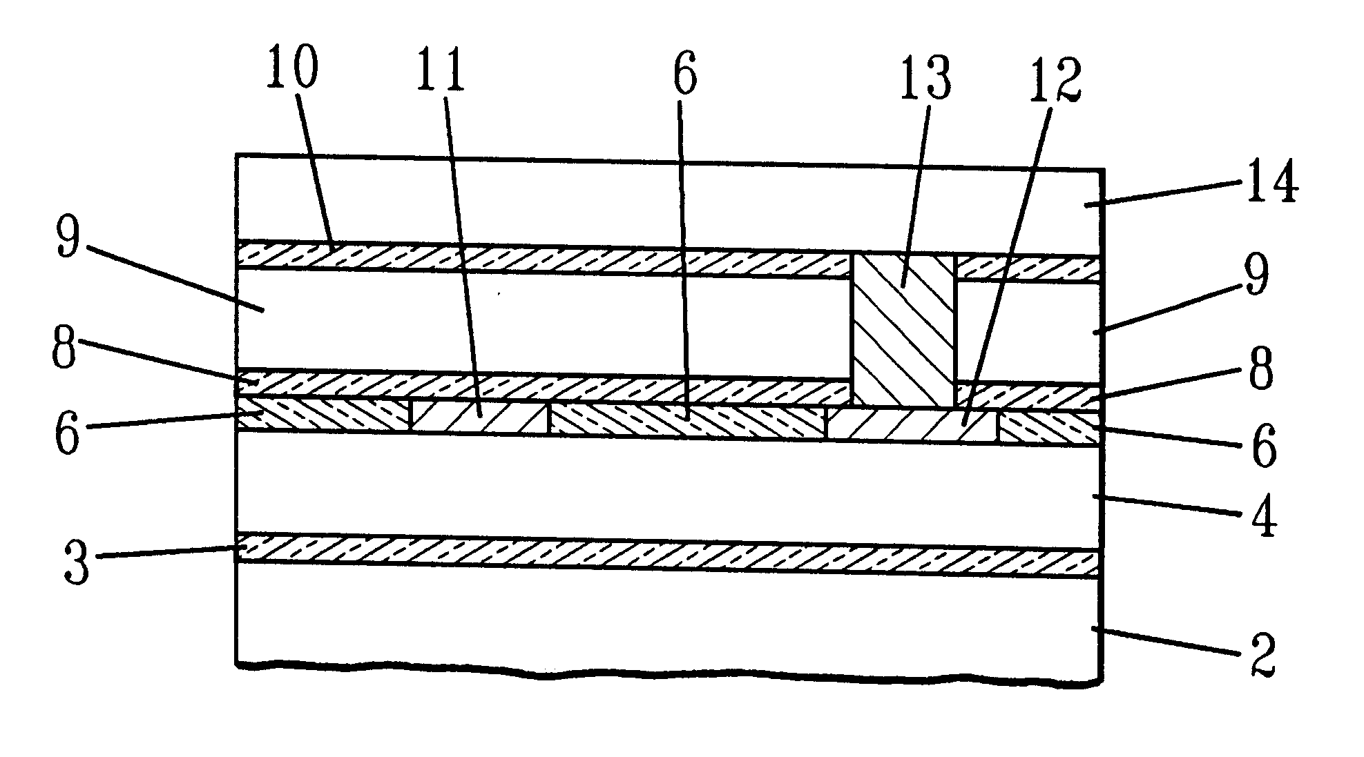
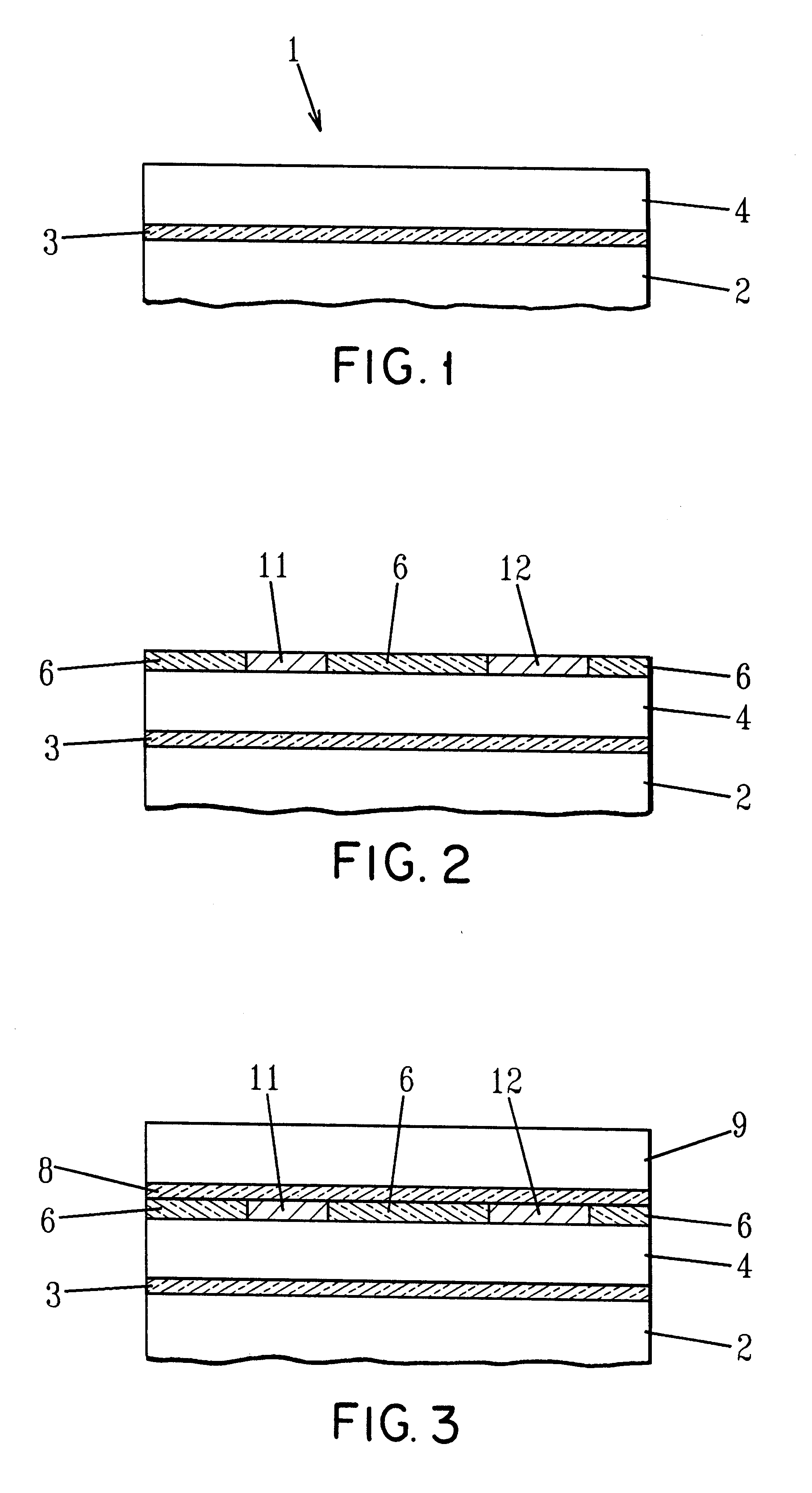
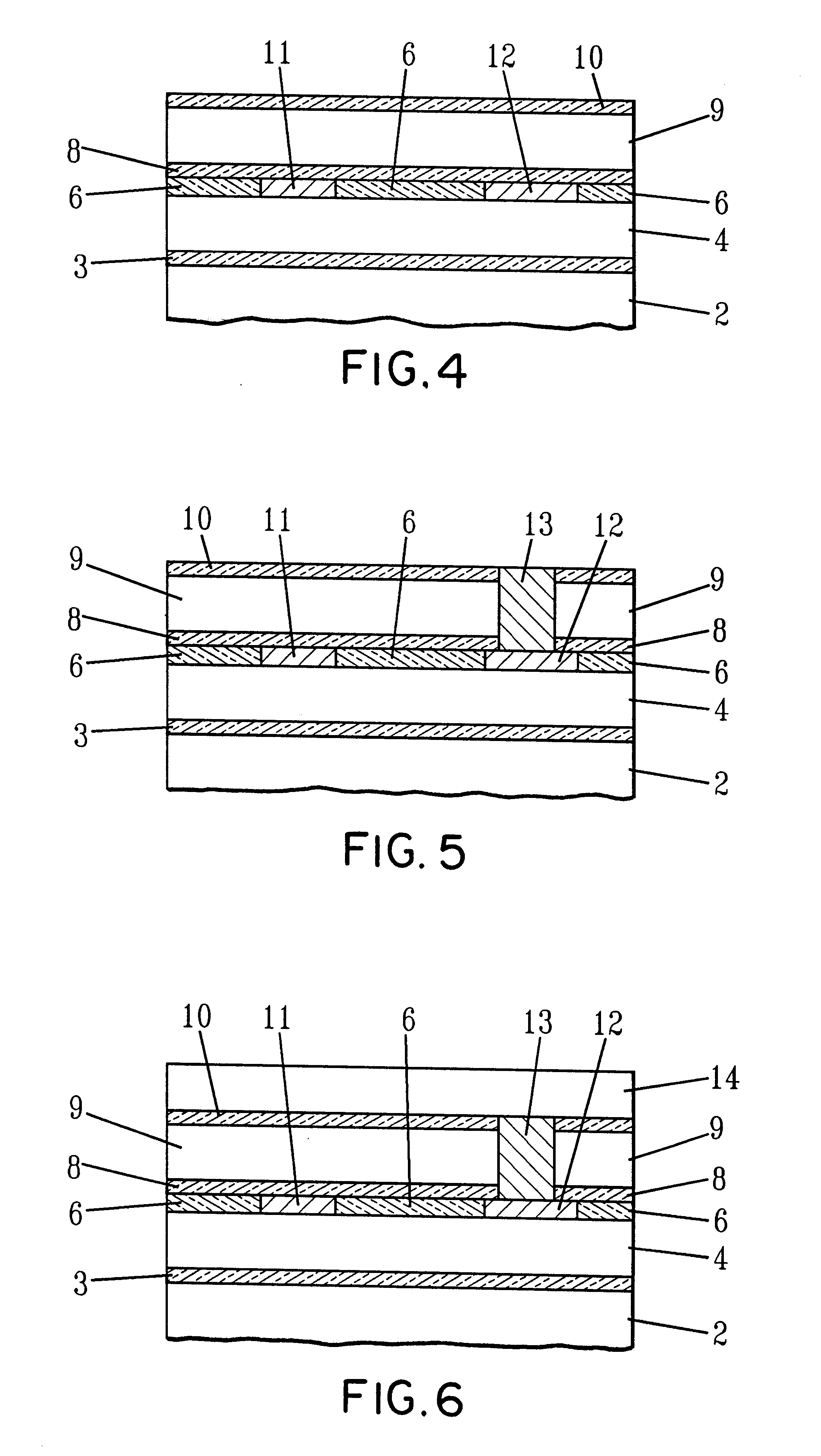
According to the present invention, a first semiconductor substrate 1 is provided. The semiconductor substrate is typically monocrystalline silicon or a SOI substrate (silicon on insulator substrate) as illustrated in FIG. 1. The SOI substrate comprises a silicon wafer 2 and an insulating layer 3 provided thereon. The insulating layer 3 can be grown on the substrate 2 or can be provided by deposition techniques such as chemical vapor deposition (CVD) or physical vapor deposition (PVD). Also, the insulating layer 3 can be provided by thermal oxidation of the substrate 2 to provide a silicon dioxide or insulating layer 3 can be provided by SIMOX or other well known methods of making SOI. Typically, this layer 3 is about 1000 to about 5000 .ANG. thick and preferably about 15...


PUM


Abstract

A multistack 3-D semiconductor structure comprising a first level structure comprising a first semiconductor substrate and first active devices; and a second level structure comprising a SOI semiconductor structure bonded to the first level structure and further comprising second active devices; and wherein the first active devices are more heat tolerant than the second active devices is provided along with a method for its fabrication.

Description

The present invention relates to multistack 3-dimensional semiconductor structures. In addition, the present invention relates to a method for fabricating the multistack 3-dimensional semiconductor structures. According to the present invention, active devices are formed on a semiconductor substrate followed by adhering a second semiconductor layer above the active devices and then building active devices on this additional semiconductor layer. The present invention makes it possible to obtain improvements in function, density and performance as compared to multistack devices previously suggested.BACKGROUND OF INVENTIONPlanar technology is principally used currently for fabricating semiconductor surfaces. The level of integration that can be achieved on a semiconductor chip is limited by the size of the chip and by the structural fineness that is obtainable. The performance of a system which is realized using planar technology and which comprises a plurality of chips connected to on...

Claims


Application Information

Patent Timeline
IPC IPC(8): H01L21/762H01L21/768H01L21/70H01L21/02H01L21/3205H01L27/00H01L23/52H01L27/12
CPCH01L21/76251H01L21/76898H01L21/76895H01L27/12
Inventor MA, WILLIAM HSIOH-LIENSCHEPIS, DOMINIC JOSEPH
Owner IBM CORP
Why Eureka
Try Eureka