
Plasma source ion implanting apparatus using the same

a technology of plasma source and ion implanting device, which is applied in the field of plasma source, can solve the problems of reducing the production yield of fabricating transistors, increasing the charge-up voltage of targets, and deteriorating product reliability

Inactive Publication Date: 2001-10-02
NISSIN ION EQUIP CO LTD
View PDF11 Cites 26 Cited by
  • Summary
  • Abstract
  • Description
  • Claims
  • Application Information

AI Technical Summary

Problems solved by technology

In carrying out a process, e.g., ion implanting process, to implant into a targets for example, a semiconductor wafer, by radiating an ion beam to the target, a problem arises in which the target is positively charged (charged up) by the positive charge of the ion beam.
Otherwise, the charge-up voltage causes the breakdown of the transistors, possibly resulting in reduction of a production yield in fabricating the transistors and deterioration of product reliability.
As a result, a problem of increase of the charge-up voltage of the target 36 arises.

Method used


Image

  • Plasma source ion implanting apparatus using the same
  • Plasma source ion implanting apparatus using the same
  • Plasma source ion implanting apparatus using the same

Examples


example

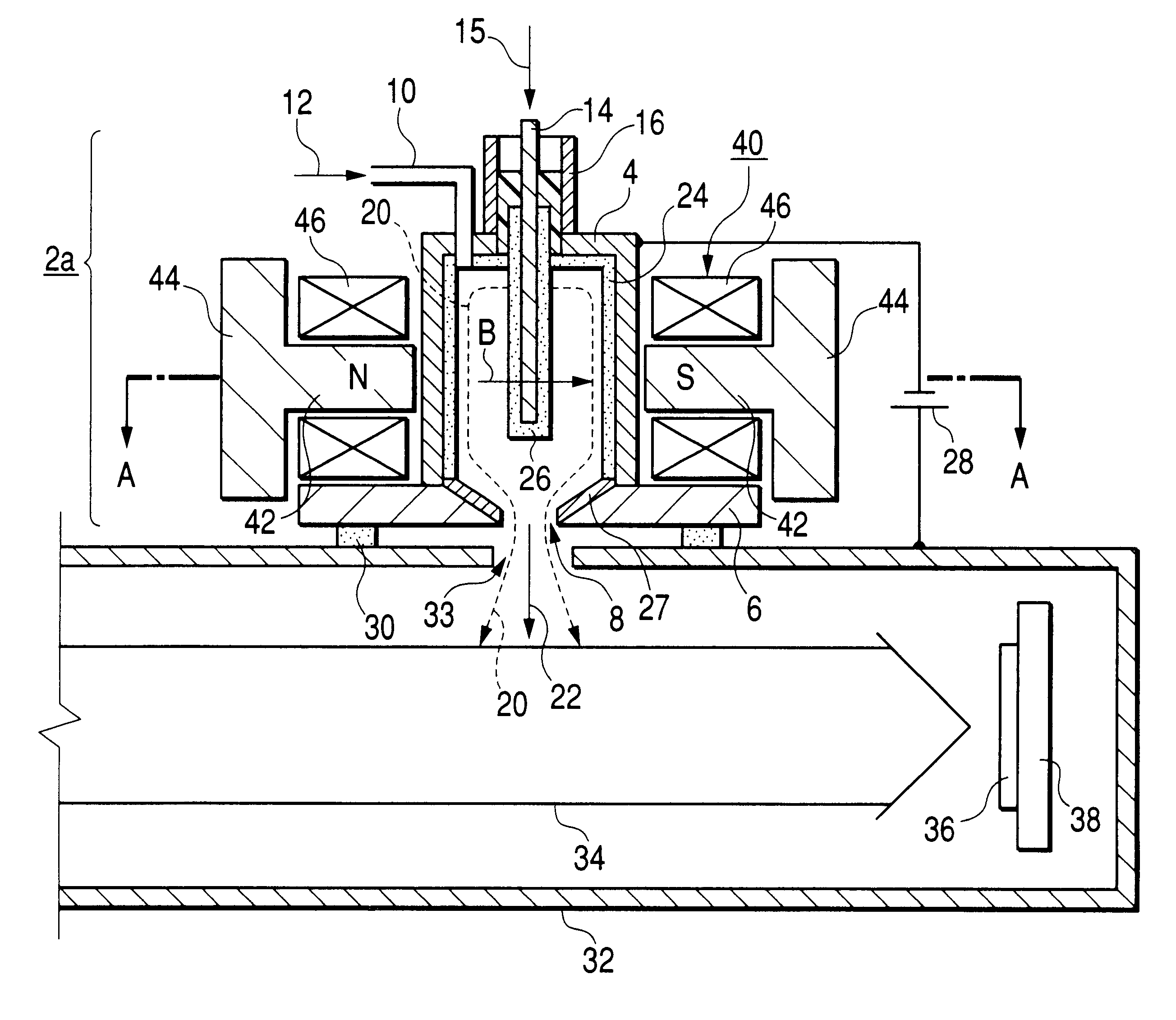
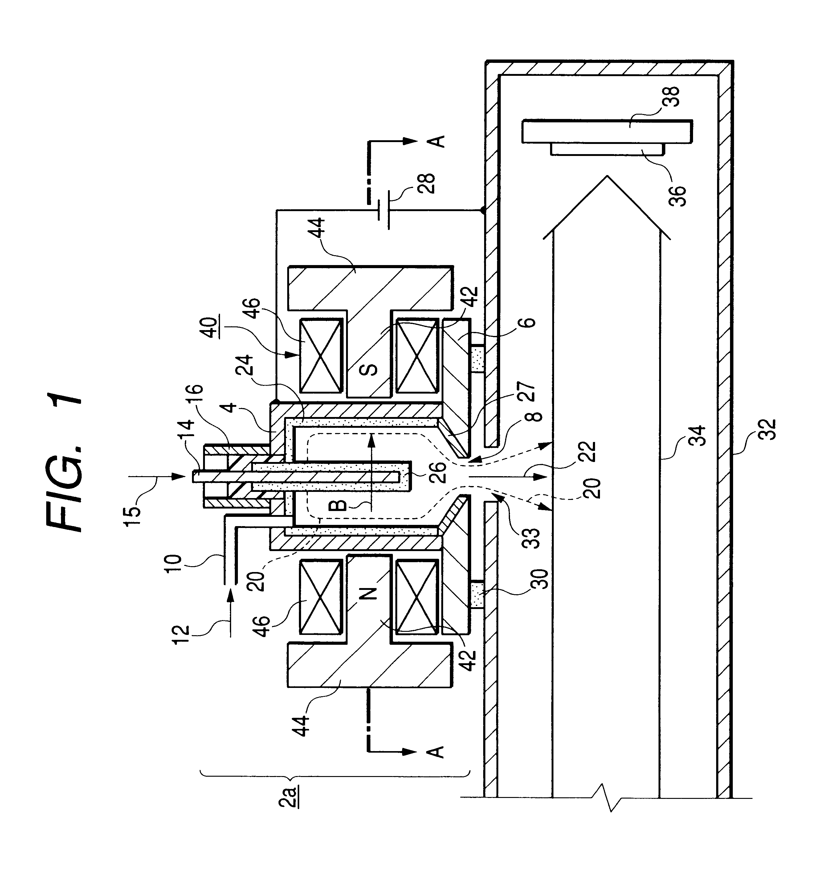
An experiment was conducted under the following conditions. The results of measuring an electron energy distribution in plasma 20 discharged from the conventional plasma source 2 shown in FIG. 6 were plotted in a graph of FIG. 4. The results of measuring an electron energy distribution in a plasma 20 generated by the plasma source 2a of the invention shown in FIG. 1 were plotted in a graph of FIG. 5. An electrostatic energy distribution analyzer was used for the measurements.

Introducing gas: xenon of 0.2 ccm

Implanting microwave power: 100 W

Extraction voltage: 30V

As seen from FIG. 4, the electron energy in the plasma 20 generated by the conventional plasma source 2 distributed over a broad range from several eV to 100 eV, and a large amount of high energy electrons exist.

On the other hand, as shown in FIG. 5, most of electron energy in the plasma 20 generated by the plasma source 2a of the invention is localized at a region of 5 eV and therearound. This tact clearly shows that the in...


PUM


Abstract

A plasma source includes a magnetic field generating unit for generating within a plasma chamber a magnetic field B for electron cyclotron resonance, which has a direction crossing a direction in which the plasma is discharged through a plasma emission aperture. The plasma source is applied to an ion implanting apparatus.

Description

1. Field of the InventionThe present invention relates to a plasma source which supplies a plasma to an ion beam and neutralizes the ion beam by electrons of the plasma to prevent the target from being charged, in an ion beam irradiation apparatus (e.g., an ion implanting apparatus) for radiating an ion beam toward a target, more particularly, relates to a means for preventing high energy electrons from being contained in the discharged plasma, and the ion implanting apparatus using the plasma source.2. Description of the Related ArtIn carrying out a process, e.g., ion implanting process, to implant into a targets for example, a semiconductor wafer, by radiating an ion beam to the target, a problem arises in which the target is positively charged (charged up) by the positive charge of the ion beam.In order to solve the charge-up problem, JP-A-5-234562 and JP-A-5-47338 disclose that a plasma source is located near a target. Plasma is supplied to an ion beam. The ion beam is neutraliz...

Claims


Application Information

Patent Timeline
IPC IPC(8): H01J37/32H01J37/317G21K5/04H01L21/265H05H1/46
CPCH01J37/32192H01J37/32357H01J37/32678H01L21/265
Inventor SAKAI, SHIGEKITAKAHASHI, MASATO
Owner NISSIN ION EQUIP CO LTD
Learn More