Methods for fabricating iii-nitride tunnel junction devices

a tunnel junction and nitride technology, applied in semiconductor/solid-state device manufacturing, semiconductor devices, electrical equipment, etc., can solve the problems of low hole concentration and mobility, inability to use p-gan as a current spreading layer, and difficulty in contact with nitride (p-gan) electrically, so as to increase efficiency, reduce the operating voltage of these devices, and increase the performance of eelds and vcsels

a tunnel junction and nitride technology, applied in semiconductor/solid-state device manufacturing, semiconductor devices, electrical equipment, etc., can solve the problems of low hole concentration and mobility, inability to use p-gan as a current spreading layer, and difficulty in contact with nitride (p-gan) electrically, so as to increase efficiency, reduce the operating voltage of these devices, and increase the performance of eelds and vcsels

US20190207043A1Active Publication Date: 2019-07-04RGT UNIV OF CALIFORNIA

Image

  • Methods for fabricating iii-nitride tunnel junction devices
  • Methods for fabricating iii-nitride tunnel junction devices
  • Methods for fabricating iii-nitride tunnel junction devices

Examples


Embodiment Construction

[0058]In the following description of the preferred embodiment, reference is made to the accompanying drawings that form a part hereof, and in which is shown by way of illustration a specific embodiment in which the invention may be practiced. It is to be understood that other embodiments may be utilized and structural changes may be made without departing from the scope of the present invention.

TECHNICAL DESCRIPTION

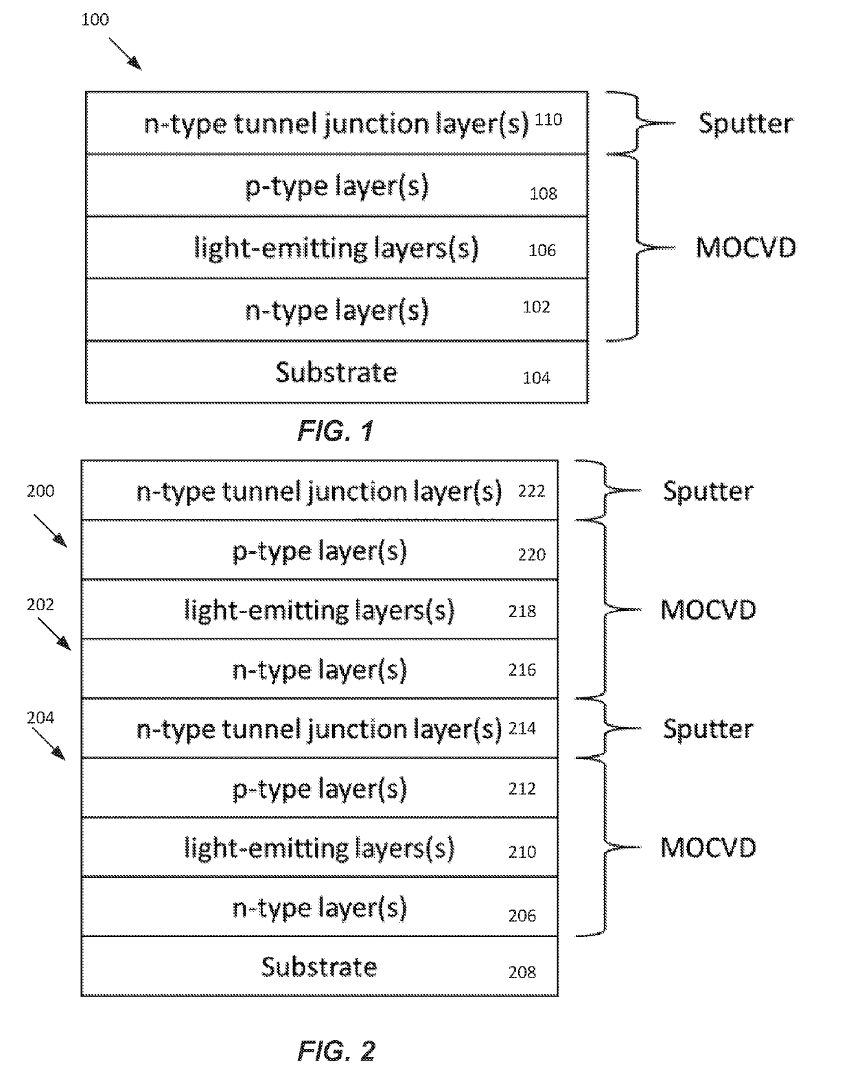
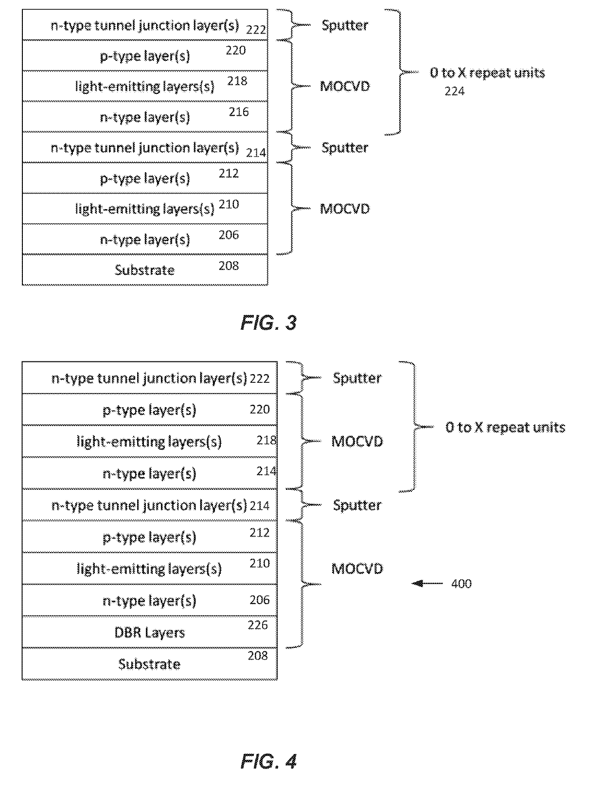
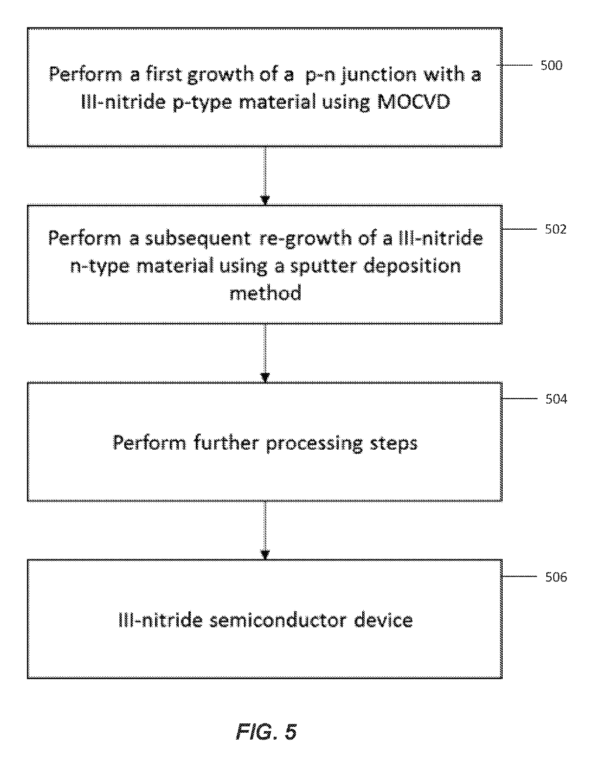
[0059]A. Physical Vapor Deposition (e.g. Sputter Deposition) Method for III-Nitride Tunnel Junction Devices

[0060]As noted above, the present invention comprises a sputter deposition method for r-nitride tunnel junction devices that uses MOCVD to grow one or more light-emitting or light-absorbing structures and sputter deposition is used to grow one or more tunnel junctions.

[0061]Tunnel junctions grown by MOCVD are difficult to achieve, because the as-grown Mg-doped layers are insulating due to hydrogen passivation, and are typically activated by a post growth anneal. If ...


PUM


Abstract

A physical vapor deposition (e.g., sputter deposition) method for III-nitride tunnel junction devices uses metal-organic chemical vapor deposition (MOCVD) to grow one or more light-emitting or light-absorbing structures and electron cyclotron resonance (ECR) sputtering to grow one or more tunnel junctions. In another method, the surface of the p-type layer is treated before deposition of the tunnel junction on the p-type layer. In yet another method, the whole device (including tunnel junction) is grown using MOCVD and the p-type layers of the III-nitride material are reactivated by lateral diffusion of hydrogen through mesa sidewalls in the III-nitride material, with one or more lateral dimensions of the mesa that are less than or equal to about 200 μm. A flip chip display device is also disclosed.

Description

CROSS REFERENCE TO RELATED APPLICATIONS[0001]This application claims the benefit under 35 U.S.C. Section 119(e) of the following co-pending and commonly-assigned applications:[0002]U.S. Provisional Patent Application No. 62 / 376,307, filed on Aug. 17, 2016, by Benjamin P. Yonkee, Asad Mughal, Steven P. DenBaars, and Shuji Nakamura, entitled “SPUTTER DEPOSITION METHOD FOR III-NITRIDE TUNNEL JUNCTION DEVICES,” Attorney's Docket No. 30794.631-US-P1 (UC Ref. 2017-130-1);[0003]U.S. Provisional Patent Application No. 62 / 376,201, filed on Aug. 17, 2016, by Benjamin P. Yonkee, Erin C. Young, James S. Speck, Steven P. DenBaars and Shuji Nakamura, entitled “III-NITRIDE TUNNEL JUNCTION IMPROVEMENT THROUGH REDUCTION OF THE MAGNESIUM MEMORY EFFECT,” Attorney's Docket No. 30794.626-US-P1 (UC Ref. 2017-134-1);[0004]U.S. Provisional Patent Application No. 62 / 491,493, filed on Apr. 28, 2017, by Asad J. Mughal, David Hwang and Steven P. DenBaars, entitled “MOCVD REGROWTH DEPOSITION METHOD FOR III-NITR...

Claims


Application Information

Patent Timeline
04 Jul 2019
Publication
US20190207043A1
IPC
H01L31/0304; H01L33/00; H01L21/02; H01L33/32
CPC
H01L31/03044; H01L33/007; H01L21/0254; H01L21/02579; H01L33/32; Y02E10/544; H01L29/207; H01L29/365
Inventors
YONKEE, BENJAMIN P.; MUGHAL, ASAD J.