

Semiconductor memory device allowing reduction in power consumption during standby
a technology power consumption, which is applied in the direction of digital storage, pulse automatic control, instruments, etc., can solve the problem of unfavorable increase in power consumption of synchronous semiconductor memory, and achieve the effect of reducing power consumption
- Summary
- Abstract
- Description
- Claims
- Application Information
AI Technical Summary
Benefits of technology
Problems solved by technology
Method used
Image

Examples
embodiment 1
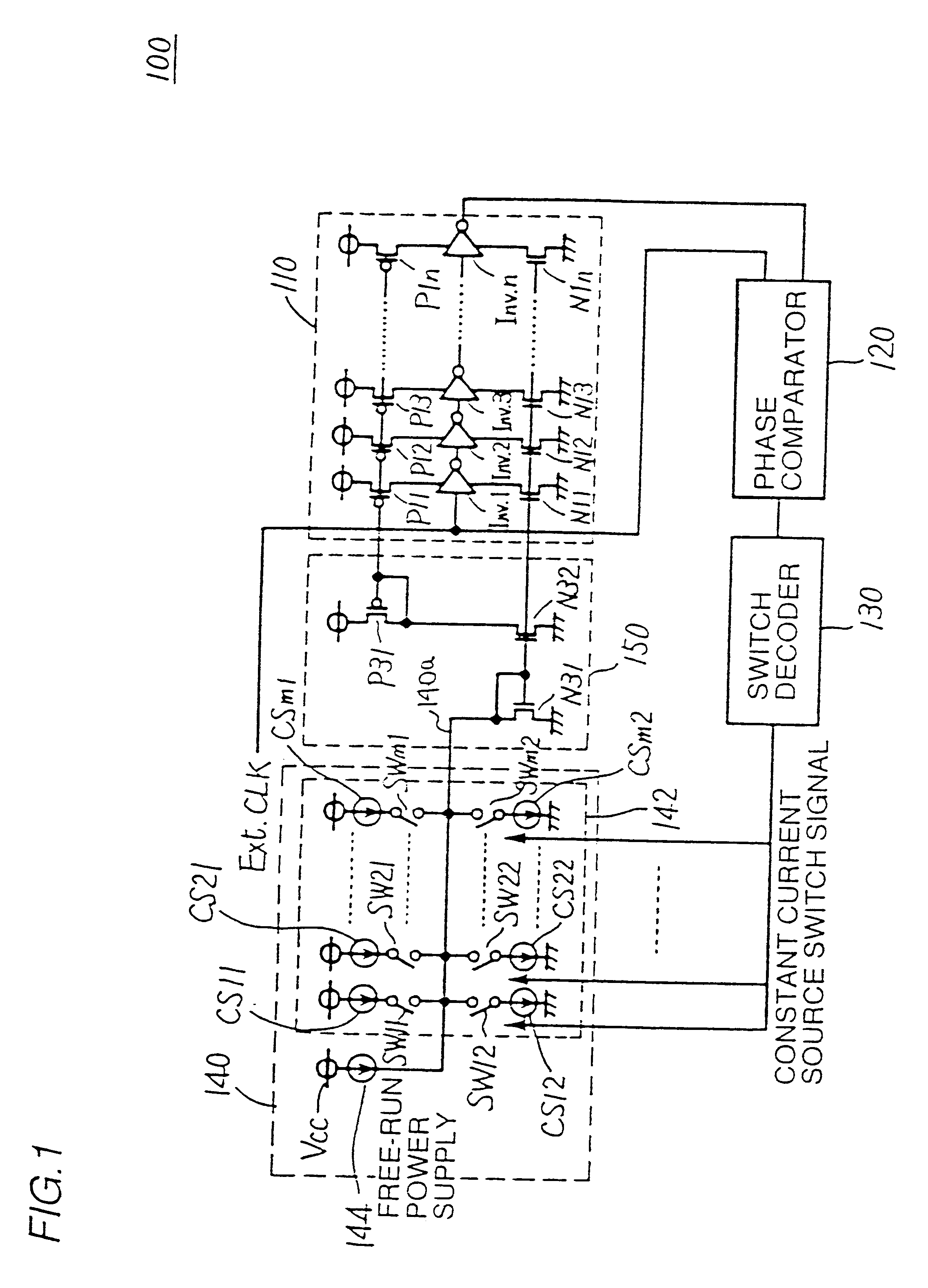
[EMBODIMENT 1]
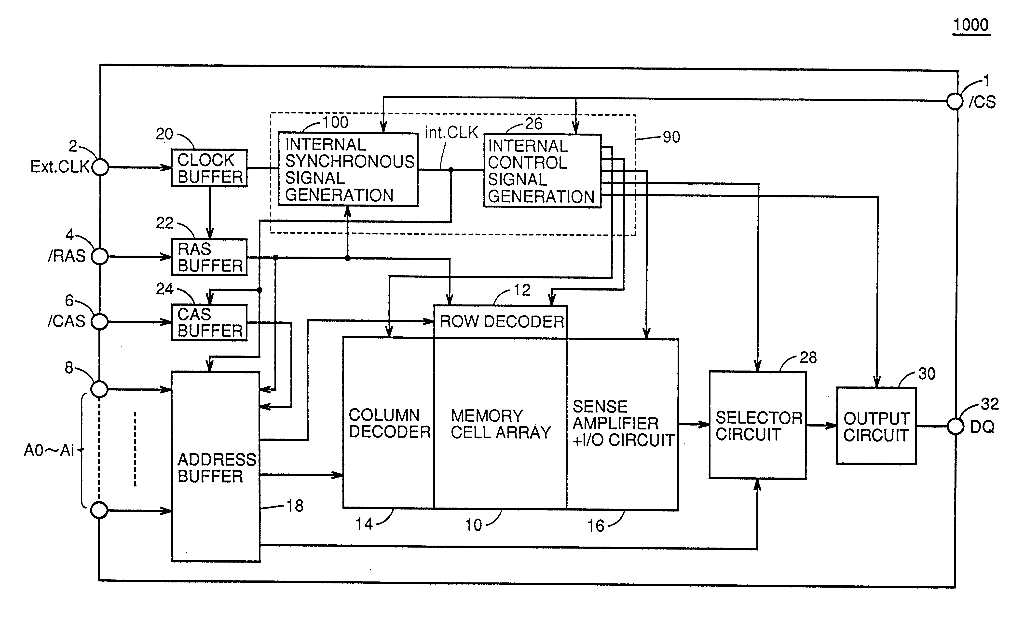
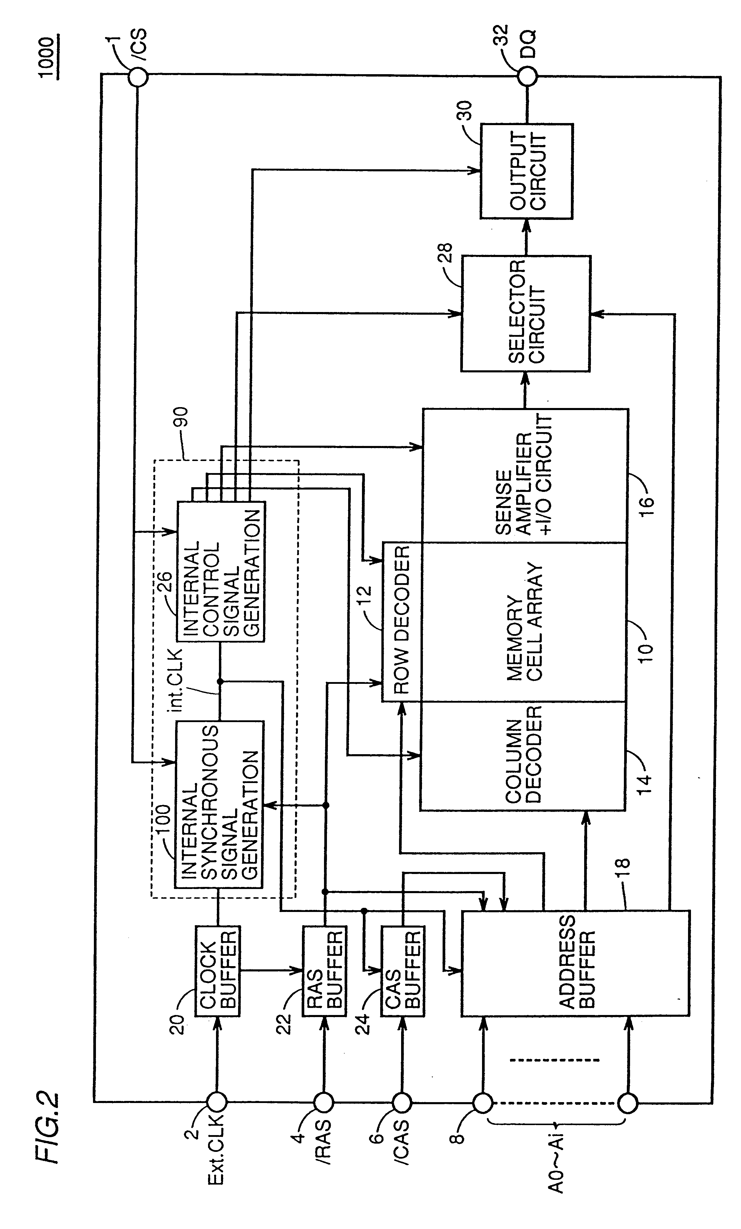
FIG. 1 is a schematic block diagram showing a structure of an internal synchronous signal generating circuit 1000 of an embodiment 1 of the invention, and FIG. 2 is a schematic block diagram showing a structure of the synchronous semiconductor memory device 1000 of the embodiment 1.
Referring to FIGS. 1 and 2, the structure of synchronous semiconductor memory device 1000 of the embodiment 1 will be described below.
Referring to FIG. 2, synchronous semiconductor memory device 1000 includes a control circuit 90, which receives external clock signal Ext.CLK and external control signals / CS, / RAS and / CAS through external control signal input terminals 1 to 8, and issues internal control signals, a memory cell array 10 having memory cells arranged in a matrix form, an address buffer 18 which receives external address signals A0-Ai through address input terminal 8, and issues an internal row address signal and an internal column address signal under the control of control cir...
embodiment 2
[Embodiment 2]
FIG. 6 is a schematic block diagram showing a structure of an internal synchronous signal generating circuit 102 of the embodiment 2 of the invention.
The structure of synchronous semiconductor memory device provided with internal synchronous signal generating circuit 102 differs from that of synchronous semiconductor memory device 1000 shown in FIG. 2 only in the internal synchronous signal generating circuit. The similar structures will not be described below.
Internal synchronous signal generating circuit 102 of the embodiment 2 includes a ring oscillator circuit 114, phase comparator 120 which receives external clock signal Ext.CLK and an output of ring oscillator circuit 114, and makes a phase comparison between them, a charge pump 180 which issues a predetermined potential in accordance with the result of comparison of phase comparator 120, an analog-digital converter circuit (i.e., A-D converter circuit) 182 which receives an output of charge pump 180 and issues c...
embodiment 3
[Embodiment 3]
FIG. 12 is a schematic block diagram showing a structure of an internal synchronous signal generating circuit 200 of an embodiment 3 of the invention.
The structure of internal synchronous signal generating circuit 200 of the embodiment 3 differs from that of internal synchronous signal generating circuit 100 of the embodiment 1 in the following two points.
First, a free-run current source 146 of the embodiment 3 can supply a current of which value is variable depending on the externally supplied control signal, although free-run power supply 144 in the embodiment 1 can supply only the free-run current of an invariable value.
Second, a command register 190 controls the value of current supplied from free-run current source 146 based on externally supplied latency data.
Structures other than the above are similar to those of internal synchronous signal generating circuit 100 of the embodiment 1. Similar portions bear the same reference numbers, and will not be described bel...
PUM
 Abstract
Description
Claims
Application Information