High performance semiconductor memory device with low power consumption

a memory device and high-performance technology, applied in semiconductor devices, digital storage, instruments, etc., can solve the problems of affecting the performance affecting the operation speed of the memory device, so as to improve the performance such as the memory access speed

Inactive Publication Date: 2001-10-23
IBM CORP
View PDF2 Cites 44 Cited by
  • Summary
  • Abstract
  • Description
  • Claims
  • Application Information

AI Technical Summary

Benefits of technology

It is an object of the present invention to provide a semiconductor memory cell employing pas...

Problems solved by technology

This is because the portable electronic devices are typically subject to the limitation of battery lifetime, i.e., a duration of usage of a battery between charges.
By lowering the supply voltage, however, operating speed of the memories is degraded such that memory access speed slows down.
In this case, however, the reduction of the threshold voltage causes an increase in subthreshold leakage current of the transistors.
The power dissipation due to the subthreshold leakage current is not negl...

Method used


Image

  • High performance semiconductor memory device with low power consumption
  • High performance semiconductor memory device with low power consumption
  • High performance semiconductor memory device with low power consumption

Examples


Embodiment Construction

Detailed illustrative embodiments of the present invention are disclosed herein. However, specific structural and functional details disclosed herein are merely representative for purposes of describing preferred embodiments of the present invention.

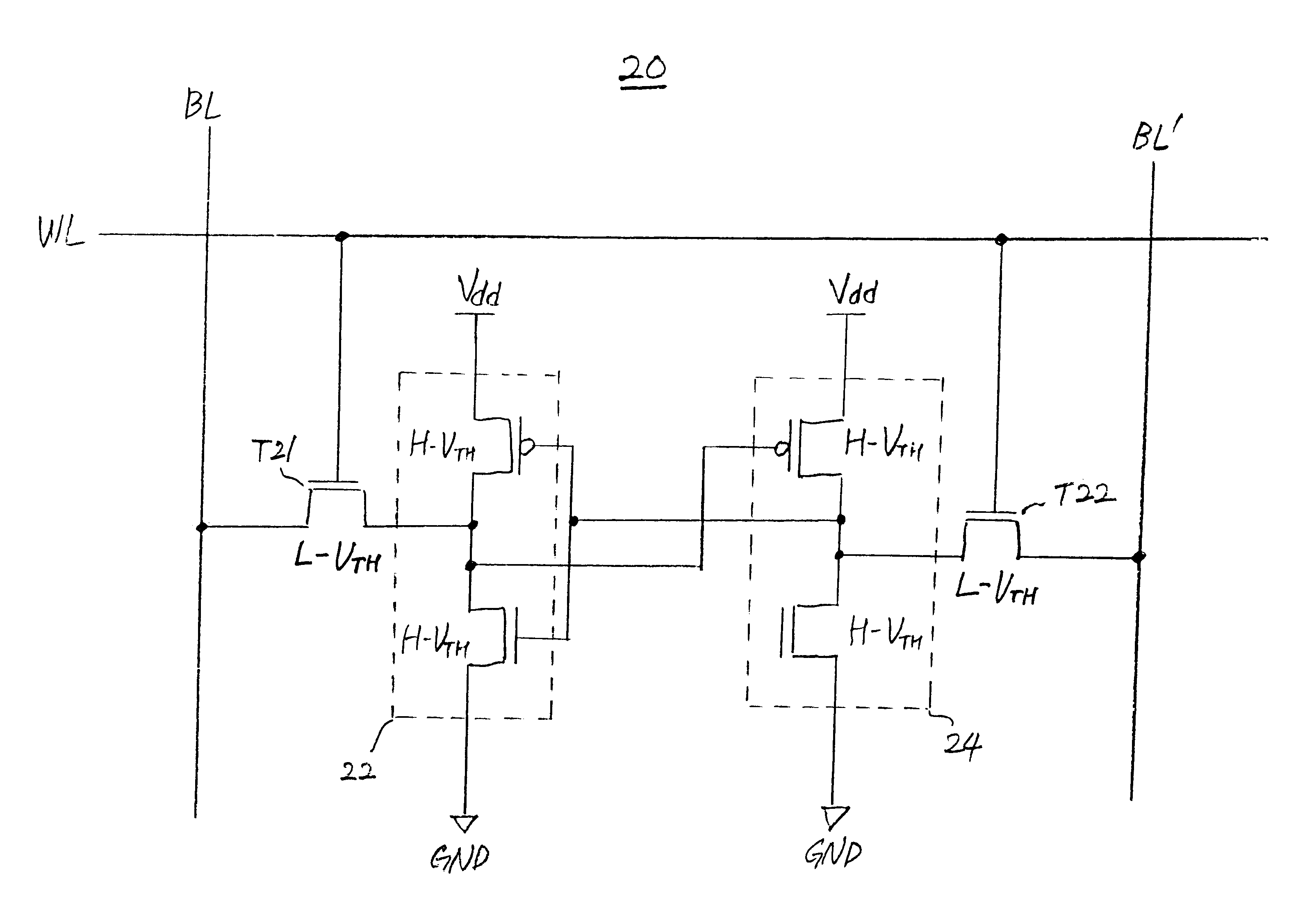
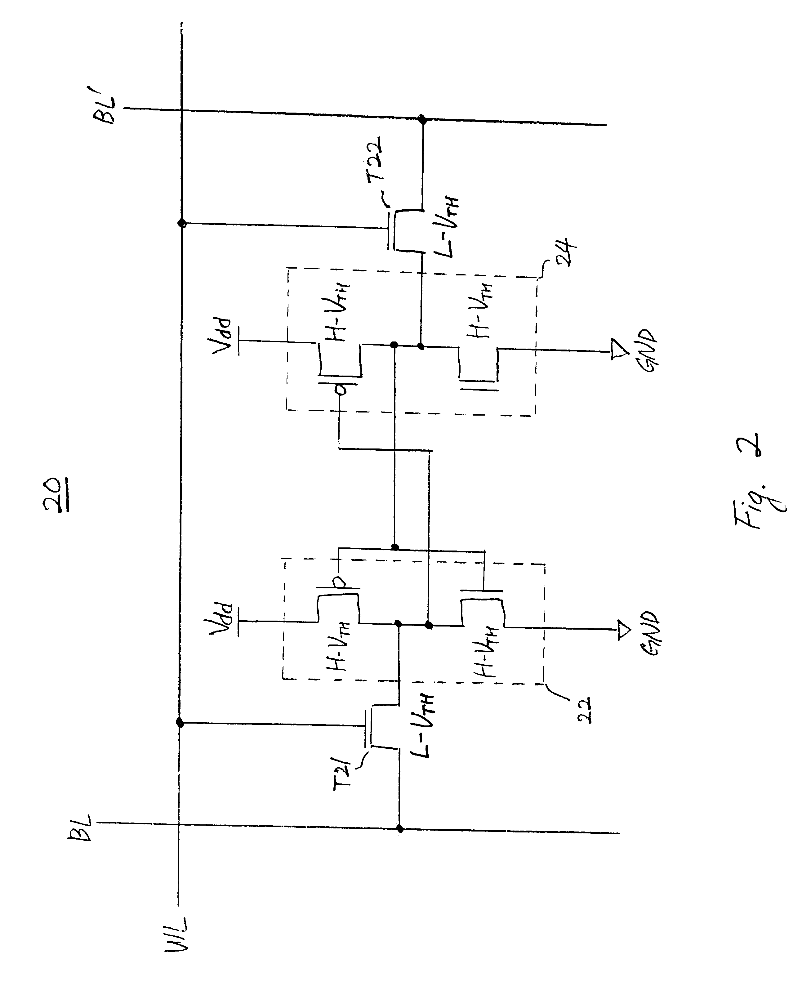
The present invention provides a semiconductor memory cell having capability of operating high performance at low supply voltage, thereby having lower power dissipation. As a preferred embodiment of the semiconductor memory cell of the present invention, a complementary metal oxide silicon (CMOS) memory cell employing multi-threshold voltage CMOS (MTCMOS) technique. It should be noted that the present invention is not limited to the CMOS memory cell. The present invention may apply to any type of memory cell which employs pass transistors to improve the performance of the memory cell and / or to a method for controlling a leakage current in a semiconductor memory cell at a standby mode.

A CMOS memory cell using the MTCMOS technique (e.g.,...


PUM


Abstract

A semiconductor memory device accessed with wordlines and bitlines has memory cells which operate at high performance with lower power consumption and have a high density. Each of the memory cells has pass transistors connected to a corresponding wordline and a corresponding pair of bitlines, and the pass transistors are gated by a signal of the corresponding wordline. The semiconductor memory device includes a wordline drive unit for selectively driving the wordlines in response to a row address. A wordline driver in the wordline drive unit boosts a corresponding wordline in a positive direction when the corresponding wordline is activated to access the memory cell and boosts the corresponding wordline in a negative direction when the corresponding wordline is inactive. By boosting the wordline in the positive direction, the performance of the memory cells is enhanced, and by boosting the wordline in the negative direction, a leakage current in the pass transistors with a low-threshold voltage is prevented.

Description

1. Field of the InventionThe present invention relates to a semiconductor memory device, and more particularly, to a semiconductor memory device having high density and capability of high performance at low supply voltage.2. Description of the Related ArtIn electronic systems, power consumption is one of the factors determining efficiency and functionality of the system. With the proliferation of wireless and portable electronic devices such as palm top computers, cellular telephones, etc., power consumption has become an important factor to be considered in designing and manufacturing such electronic devices. This is because the portable electronic devices are typically subject to the limitation of battery lifetime, i.e., a duration of usage of a battery between charges. Thus, in battery operated portable electronic devices, there have been efforts to reduce the power consumption of the devices which is an important factor determining the battery lifetime.For semiconductor memories...

Claims


Application Information

Patent Timeline
IPC IPC(8): G11C11/418G11C8/08G11C8/00H01L27/11
CPCG11C8/08G11C11/418H01L27/11H10B10/00
Inventor ANDERSEN, JOHN E.HOOK, TERENCE B.HSU, LOUIS L.HWANG, WEIKOSONOCKY, STEPHEN V.WANG, LI-KONG
Owner IBM CORP
Why Eureka
Try Eureka